Midas Passive OLED Part Number System
|
|
|
- Ἰαρέδ Λούπης
- 7 χρόνια πριν
- Προβολές:
Transcript


1
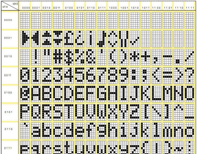
2 Midas Passive OLED Part Number System MC OC 57/265 A W * M Y * = MC: Midas Components 2 = OC: OLED Character OG: OLED Graphic 3 = Size / No of Characters and Character Height 4 = Series 5 = Operating Temp Range: B: -4+7Deg C W: -4+8 Deg C 6 = Blank:Not applicable or No of Pixels (3224) 7 = Mode: M: Transmissive S: Sunlight Readable (transmissive) 8 = Colour: Y: Yellow G: Green R: Red B: Blue W: White RGB: Red, Green, Blue 9 = Driver Chip/Controller: Blank: General I: I 2 C E: Multi-European Character Set
3 Version Contents Date Note NEW VERSION 22/6/8 Spec. Update Power up Sequence 22/6/25 Spec.
4 MODULE CLASSIFICATION INFORMATION... 2 HISTORY OF VERSION... 3 ()DIMENSION... 5 (2)ABSOLUTE MAXIMUMRATING ELECTRICAL ABSOLUTE RATINGS ENVIRONMENTAL ABSOLUTE MAXIMUM RATINGS...6 (3)ELECTRICAL CHARACTERISTICS... 7 (4)OPTICAL CHARACTERISTICS... 7 (5)MECHANICAL SPECIFICATION... 8 (6)INTERFACE PIN ASSIGNMENT... 8 (7) I 2 C INTERFACE: (FOR I 2 C MODEL)... 9 (8)BLOCK DIAGRAM (9)POWER SUPPLY...PLY ()FUNCTIONAL SPECIFICATION... I.... TABLE -: FUNDAMENTAL COMMAND MAND TABLE TABLE -2: EXTENDED COMMAND TABLE...4 TABLE -3: OLED COMMAND TABLE...5 ()POWER DOWN AND POWER UP SEQUENCE...7 (2) 68-SERIES MCU PARALLEL INTERFACE TIMING CHARACTERISTICS...8 (3)APPLICATION...2 (4)SSD3 CGROM CHARACTER CODE...22 (5)PRECAUTIONS IN USE OF OLED MODULES MODULES...25 HANDLING PRECAUTIONS...25 STORAGE PRECAUTIONS...26 DESIGNING PRECAUTIONS...26 (6)PRECAUTIONS IN USE OF OLED MODULES PRECAUTIONS WHEN DISPOSING OF THE OLED DISPLAY MODULES...27 OTHER PRECAUTIONS...27
5 ()Dimension FH62BW Ver.
6 (2)ABSOLUTE MAXIMUMRATING 2. Electrical Absolute Ratings Item Symbol Min. Typ. Max. Unit Notes 2.2 Environmental Absolute Maximum Ratings Wide Temperature re Item Operating Storage Min Max. Min, Max. Note : The defined temperature ranges do not include the polarizer. The maximum withstood temperature of the polarizer should be 85C.
7 (3)ELECTRICAL CHARACTERISTICS Item Symbol Condition Min. Typ Max. Unit μ (4)OPTICAL CHARACTERISTICS Item Symbol Min. Typ Max. Unit
8 (5)MECHANICAL SPECIFICATION Item Description MCOC22AWMGE (6)INTERFACE PIN ASSIGNMENT Pin No. Symbol External Connection Description ion 68interface: 88interface: 68interface: 88interface:
9 (7) I 2 C INTERFACE: (FOR I 2 C MODEL) Pin No. Symbol External Connection Description
10 (8)BLOCK DIAGRAM (9)POWER SUPPLY
 D7 D6 D5 D4 D3 D2 D D Clear Display Return Home X X X * Description Write \"2H\" to DDRAM and set DDRAM address to \"H\" from AC.")
 X I/D S I/D = \"\": cursor/ blink moves to left and DDRAM address d is decreased by Assign display shift with DDRAM")
11 ()FUNCTIONAL SPECIFICATION COMMAND TABLE Table -: Fundamental Command Table. Fundamental Command Set Instruction Code Command IS RE SD D/C# R/W# (WR#) D7 D6 D5 D4 D3 D2 D D Clear Display Return Home X X X * Description Write "2H" to DDRAM and set DDRAM address to "H" from AC. Set DDRAM address to "H" from AC and return cursor to its original position if shifted. The contents of DDRAM are not changed. Assign cursor / blink moving direction with DDRAM address. I/D = "": cursor/ blink moves to right and DDRAM address is increased by (POR) X I/D S I/D = "": cursor/ blink moves to left and DDRAM address d is decreased by Assign display shift with DDRAM address. dr s. Entry Mode Set S = "": make display shift of the enabled lines by the DS4 to DS bits in the shift enable instruction. Left/ right direction depends on I/D bit selection. X BDC BDS S = "": display shift disable (POR) Common bi-direction function. BDC = "": COM3 -> COM BDC = "": COM -> COM3 Segment bi-direction function. BDS = "": SEG99 -> SEG, BDS = "": SEG -> SEG99 Set display/cursor/blink ON/OFF D = "": display ON, D = "": display OFF (POR), Display ON / OFFControl X D C B C = "": cursor ON, C = "": cursor OFF (POR), B = "": blink ON, B = "": blink OFF (POR). Note: It is recommended to turn off the cursor and blinking effects when updating internal RAM contents for better visual performance;
12 . Fundamental Command Set Instruction Code Command IS RE SD D/C# R/W# D7 D6 D5 D4 D3 D2 D D Description Assign font width, black/white inverting of cursor, and 4-line display mode control bit. FW = "": 6-dot font width, FW = "": 5-dot font width (POR), Extended Function Set X FW B/W NW B/W = "": black/white inverting of cursor enable, B/W = "": black/white inverting of cursor disable (POR) NW = "": 3-line or 4-line display mode (POR) NW = "": -line or 2-line display mode Cursor or Display Shift Double Height (4- line) / Display-dot shift S/C R/L * * UD2 UD * DH Set cursor moving and display shift control bit, and the direction, without changing DDRAM data. S/C = "": display shift, S/C = "": cursor shift, R/L = "": shift to right, R/L = "": shift to left UD2~: Assign different doubt height format (POR=b) b) DH = "": display shift enable DH = "": dot scroll enable (POR) DS[4:]=b (POR) when DH =b Determine the line for display shift. Shift Enable DS4 DS3 DS2 DS DS = "/": st line display shift enable/disable DS2 = "/": 2 nd line display shift enable/disable DS3 = "/": 3 rd line display shift enable/disable DS4 = "/": 4 th line display shift enable/disable. Scroll Enable HS4 HS3 HS2 HS HS[4:]=b (POR) when DH =b Determine the line for horizontal smooth scroll. HS = "/": st line dot scroll enable/disable HS2 = "/": 2 nd line dot scroll enable/disable HS3 = "/": 3 rd line dot scroll enable/disable HS4 = "/": 4 th line dot scroll enable/disable.
13 . Fundamental Command Set Instruction Code Command IS RE SD D/C# R/W# D7 D6 D5 D4 D3 D2 D D Description Numbers of display line, N when N = "" (POR): 2-line (NW=b) / 4-line (NW=b), when N = "": -line (NW=b) / 3-line (NW=b) X * N DH RE () IS DH = /: Double height font control for 2-line mode enable/ disable (POR=) Extension register, RE ("") Function Set Extension register, IS X * N BE RE () CGRAM blink enable BE = b: CGRAM blink enable BE = b: CGRAM blink disable (POR) REV Extension register, RE ("") Reverse bit REV = "": reverse display, REV = "": normal display (POR) Set CGRAM address Set DDRAM Address Set Scroll Quantity AC5 AC4 AC3 AC2 AC AC X AC6 AC5 AC4 AC3 AC2 AC AC X * SQ5 SQ4 SQ3 SQ2 SQ SQ Set CGRAM address in address counter. (POR= ) ) ) Set DDRAM address in address counter. (POR= ) ) Set the quantity of horizontal dot scroll. (POR= ) Valid up to SQ[5:] = b Read Busy Flag and Address/ Part ID X X BF AC6 / ID6 AC5 / ID5 AC4 / ID4 AC3 / ID3 AC2 / ID2 AC / ID AC / ID Can be known whether during internal operation or not by reading BF. The contents of address counter or the part ID can also be read. When it is read the first time, the address counter can be read. When it is read the second time, the part ID can be read. BF = "": busy state BF = "": ready state Write data X X D7 D6 D5 D4 D3 D2 D D Read data X X D7 D6 D5 D4 D3 D2 D D Write data into internal RAM (DDRAM / CGRAM ). Read data from internal RAM (DDRAM / CGRAM ).
 Hex D7 D6 D5")
![D4 D3 D2 D D X 7 A[7:] = h, Disable internal V DD X A[7:] A 7 A 6 A 5 A 4 A 3 A 2 A A regulator](/docs-images/86/93236113/images/14-1.jpg "at 5V I/O application mode Function Selection A A[7:] = 5Ch, Enable internal V DD regulator at 5V")
![I/O application mode (POR) X X 72 * * * * OP[:]: Select the character no.](/docs-images/86/93236113/images/14-2.jpg "of RORO OP OP character generator OP[:] CGROM CGRAM b 24 8 b 248 8 b 25 6 b 256 Function")
![Selection B RO[:]: Select character ROM RO[:] ROM b A b B b C b Invalid Note: It is recommended](/docs-images/86/93236113/images/14-3.jpg "to turn off the disply (cmd 8h) before setting no.")

14 Table -2: Extended Command Table 2. Extended Command Set IS RE SD Instruction Code Command Description D/C# R/W# (WR#) Hex D7 D6 D5 D4 D3 D2 D D X 7 A[7:] = h, Disable internal V DD X A[7:] A 7 A 6 A 5 A 4 A 3 A 2 A A regulator at 5V I/O application mode Function Selection A A[7:] = 5Ch, Enable internal V DD regulator at 5V I/O application mode (POR) X X 72 * * * * OP[:]: Select the character no. of RORO OP OP character generator OP[:] CGROM CGRAM b 24 8 b b 25 6 b 256 Function Selection B RO[:]: Select character ROM RO[:] ROM b A b B b C b Invalid Note: It is recommended to turn off the disply (cmd 8h) before setting no. of CGRAM and defining character ROM, while clear display (cmd h) is recommended to sent afterwards OLED Characterization X X 78 /79 SD Extension register, SD SD = b: OLED command set is disabled (POR) SD = b: OLED command set is enabled Details refer to Table -3. Notes () POR stands for Power On Reset Values. (2) * and X stand for Don t care.
15 Table -3: OLED Command Table 3. OLED Command Set Command IS RE SD Instruction Code Descri Set Contrast Control Set Display Clock Divide Ratio/Oscillator Frequency X X X X D/C# R/W# (WR#) Hex D7 D6 D5 D4 D3 D2 D D 8 A[7:] D5 A[7:] ption A 7 A 6 A 5 A 4 A 3 A 2 A A Double byte command to select out of 256 contrast steps. Contrast increases as the value increases. (POR = 7Fh ) A 7 A 6 A 5 A 4 A 3 A 2 A A A[3:] : Define the divide ratio (D) of the display clocks (DCLK): Divide ratio= A[3:] + (POR=b) A[7:4] : Set the Oscillator Frequency, F OSC. Oscillator Frequency increases with the value of A[7:4] and vice versa. (POR=b) Set Phase Length Set SEG Pins Hardware Configuration X X D9 A[7:] Range:b~b A[3:] : Phase period of up to 32 A 7 A 6 A 5 A 4 A 3 A 2 A A DCLK; clock is an valid entry with 2 DCLK (POR=b) A[7:4] : Phase 2 period of up to 5 DCLK; clock is invalid entry (POR=b) X DA A[4]=b, Sequential SEG pin X A[5:4] A 5 A 4 configuration A[4]=b (POR), Alternative (odd/even) SEG pin configuration A[5]=b (POR), Disable SEG Left/Right remap A[5]=b, Enable SEG Left/Right remap Refer to Table 8-4 for details Set V COMH Deselect Level X X DB A[6:4] A 6 A 5 A 4 A[6:4] Hex V COMH deselect code b h level ~.65 x V CC b h ~.7 x V CC b 2h ~.77 x V CC b 3h (POR) ~.83 x V CC b 4h xv CC
![3. OLED Command Set Command IS RE SD Instruction Code Description D/C# R/W# (WR#) Hex D7 D6 D5 D4 D3 D2 D D X DC Set VSL & GPIO X A[7:] A7](/docs-images/86/93236113/images/16-0.jpg "A A Set VSL: A[7] = b: Internal VSL (POR) A[7] = b: Enable external VSL Function Selection C Set GPIO: A[:] = b represents GPIO pin HiZ,")
![input disabled (always read as low) A[:] = b represents GPIO pin HiZ, input enabled A[:] = b represents GPIO pin output Low (RESET) A[:] =](/docs-images/86/93236113/images/16-1.jpg "b represents GPIO pin output High X X 23 A[5:] * * A[5:4] = b Disable Fade Out / A 5 A 4 A 3 A 2 A A Blinking Mode[RESET] A[5:4] = b")


![A[3:] : Set time interval for each fade step A[3:] Time interval for each fade step b 8Frames b 6 Frames b 24 Frames : : b 2 Frames b 28](/docs-images/86/93236113/images/16-4.jpg "Frames Note () POR stands for Power On Reset Values. (2) * and X stand for Don t care.")
16 3. OLED Command Set Command IS RE SD Instruction Code Description D/C# R/W# (WR#) Hex D7 D6 D5 D4 D3 D2 D D X DC Set VSL & GPIO X A[7:] A7 A A Set VSL: A[7] = b: Internal VSL (POR) A[7] = b: Enable external VSL Function Selection C Set GPIO: A[:] = b represents GPIO pin HiZ, input disabled (always read as low) A[:] = b represents GPIO pin HiZ, input enabled A[:] = b represents GPIO pin output Low (RESET) A[:] = b represents GPIO pin output High X X 23 A[5:] * * A[5:4] = b Disable Fade Out / A 5 A 4 A 3 A 2 A A Blinking Mode[RESET] A[5:4] = b Enable Fade Out mode. Once Fade Mode is enabled, contrast decrease gradually to all pixels OFF. Output follows RAM content when Fade mode is disabled. Set Fade Out and Fade in / out A[5:4] = b Enable Fade in / out mode. Once Fade in / out mode is enabled, contrast decrease gradually to all pixels OFF and than contrast increase gradually to normal display. This process loop continuously until the Fade in / out mode is disabled. A[3:] : Set time interval for each fade step A[3:] Time interval for each fade step b 8Frames b 6 Frames b 24 Frames : : b 2 Frames b 28 Frames Note () POR stands for Power On Reset Values. (2) * and X stand for Don t care. (3) The locked OLED driver IC MCU interface prohibits all commands access except logic bit SD is set to b. (4) Refer to Table - and Table -2 for the details of logic bits IS, RE and SD.
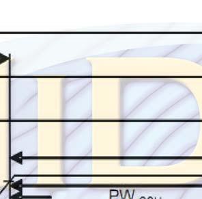
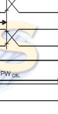
17 ()Power down and Power up Sequence Display off V off V off Reset Circuit
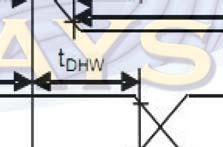
18 (2) 68-Series MCU Parallel Interface Timing Characteristics Symbol Descripti Min Max Unit

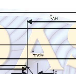

19 Note : 68-Series


20 (3)Application VDD/VCC off State Set Pre-Charge Period xd9, xf Set VCOMH Deselect Level xdb, x4 Exiting Set OLED Characterization x78, x28 Clear Display x Set Segment en Low Voltage & GPIO xdc, x3 3 Set DDRAM Address x8 Initial Settings tings Configuration o Set Display On xc Set Contrast Control x8, xff Display Data Sent
 x2a(c), x79(c), xdc(c) C), X2(C) Sleep Mode Disable Internal Regulator x2a (C),x79")
 Power up VCC (ms Delay Recommended) Set Display On x78 (C), x28 (C),xC (C) Normal")
21 Normal Operation Set Display Off x78(c), x28(c), x8(c) Sleep Mode Power down VCCV (GPIO) O) x2a(c), x79(c), xdc(c) C), X2(C) Sleep Mode Disable Internal Regulator x2a (C),x79 (C),x7 (C) x5c (D),xDC (C),x3 (C) Disable Internal nal Regulator x2a(c), x7(c) x(d), x28(c) Power up VCC (ms Delay Recommended) Set Display On x78 (C), x28 (C),xC (C) Normal Operation


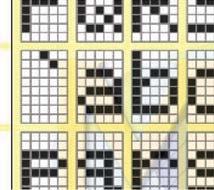
22 (4)SSD3 CGROM CHARACTER CODE ROMA

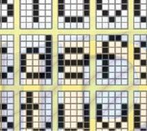

23 ROMB
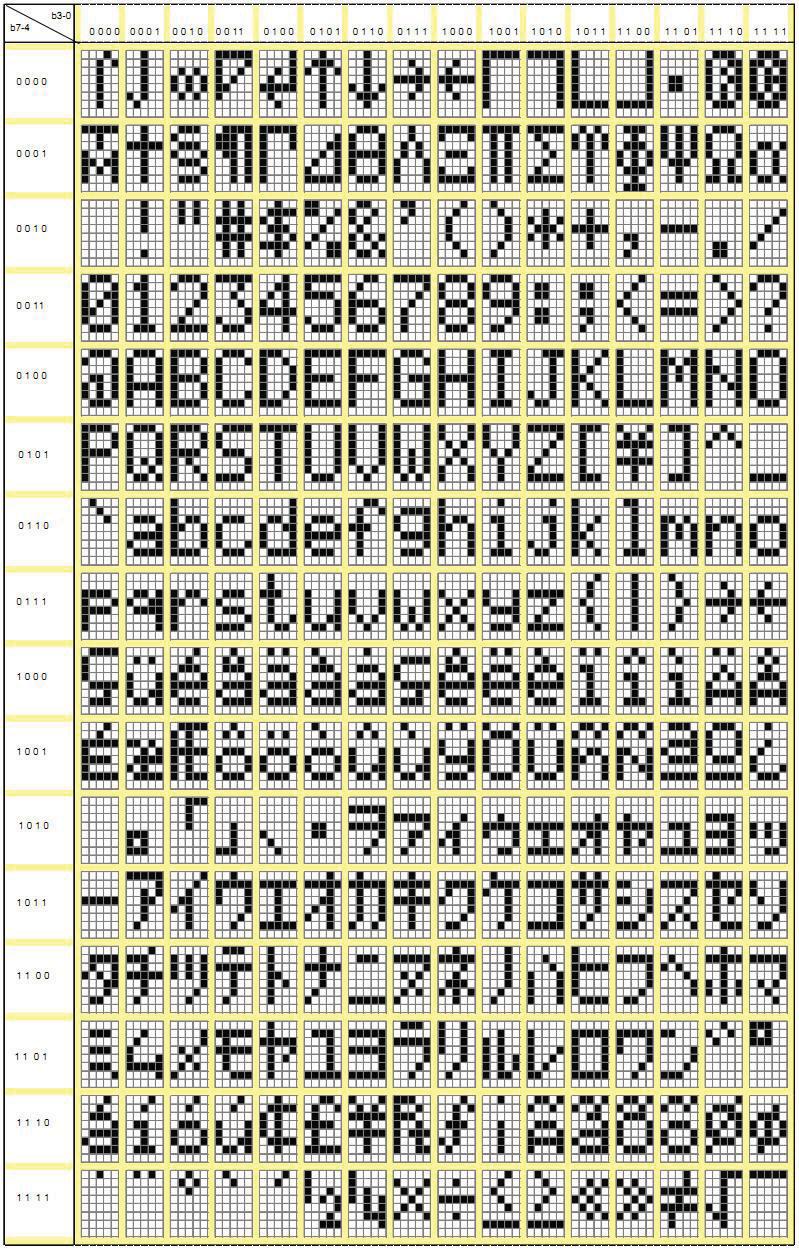
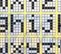
24 ROMC

25 (5)Precautions in use of OLED Modules-
26 IC.
27 (6)Precautions in use of OLED Modules-2
DC-DC Constant Current Step-Down LED driver LDD-300L LDD-350L LDD-500L LDD-600L LDD-700L CURRENT RANGE
 SPECIFICATION ORDER NO. LDD-00L LDD-0L LDD-00L LDD-00L LDD-700L CURRENT RANGE 00mA 0mA 00mA VOLTAGE RANGE Note. ~ VDC for LDD-00~700L/LW ; ~ 8VDC for LDD-00~700LS CURRENT ACCURACY (Typ.) ±% at VDC input
DC-DC Constant Current Step-Down LED driver LDD-300L LDD-350L LDD-500L LDD-600L LDD-700L CURRENT RANGE
 SPECIFICATION ORDER NO. LDD-00L LDD-0L LDD-00L LDD-00L LDD-700L CURRENT RANGE 00mA 0mA 00mA 00mA VOLTAGE RANGE Note. ~ VDC for LDD-00~700L/LW ; ~ 8VDC for LDD-00~700LS CURRENT ACCURACY (Typ.) ±% at VDC
BM1385. Bitcoin Hash ASIC Datasheet. Bitmain Technologies Limited
 BM1385 Bitcoin Hash ASIC Datasheet Bitmain Technologies Limited Page 1 of 14 Contents Contents... 1 Revision History... 2 1 Overview... 3 1.1 Features... 3 1.2 Applications... 3 2 Pin Description... 4
Metal Oxide Varistors (MOV) Data Sheet
 Data Sheet") Φ SERIES Metal Oxide Varistors (MOV) Data Sheet Features Wide operating voltage (V ma ) range from 8V to 0V Fast responding to transient over-voltage Large absorbing transient energy capability Low clamping
Φ SERIES Metal Oxide Varistors (MOV) Data Sheet Features Wide operating voltage (V ma ) range from 8V to 0V Fast responding to transient over-voltage Large absorbing transient energy capability Low clamping
Rating to Unit ma ma mw W C C. Unit Forward voltage Zener voltage. Condition
 MA MA Series Silicon planer e For stabilization of power supply ø.56. Unit : mm Features Color indication of VZ rank classification High reliability because of combination of a planer chip and glass seal
! " # $ &,-" " (.* & -" " ( /* 0 (1 1* 0 - (* 0 #! - (#* 2 3( 4* 2 (* 2 5!! 3 ( * (7 4* 2 #8 (# * 9 : (* 9
 "# " # $ "%%" & '" (' )' * & + (' )' * &,-" " (.* & -" " ( /* 0 (1 1* 0 - (* 0 # - (#* 2 # - (#* 2 3( 4* 2 (* 2 5 3 ( * 2 6 3 (7 4* 2 #8 (# * 9 : (* 9 #" " 5,1 < = " = #+ +# 9 ' :> # &? + # & ISD i " @
65W PWM Output LED Driver. IDLV-65 series. File Name:IDLV-65-SPEC
 ~ A File Name:IDLV65SPEC 07050 SPECIFICATION MODEL OUTPUT OTHERS NOTE DC VOLTAGE RATED CURRENT RATED POWER DIMMING RANGE VOLTAGE TOLERANCE PWM FREQUENCY (Typ.) SETUP TIME Note. AUXILIARY DC OUTPUT Note.
RSDW08 & RDDW08 series
 /,, MODEL SELECTION TABLE INPUT ORDER NO. INPUT VOLTAGE (RANGE) NO LOAD INPUT CURRENT FULL LOAD VOLTAGE CURRENT EFFICIENCY (Typ.) CAPACITOR LOAD (MAX.) RSDW08F-03 344mA 3.3V 2000mA 80% 2000μF RSDW08F-05
15W DIN Rail Type DC-DC Converter. DDR-15 series. File Name:DDR-15-SPEC
 DIN Rail Type DC-DC Converter ± : DIN Rail Type DC-DC Converter SPECIFICATION MODEL OUTPUT INPUT PROTECTION ENVIRONMENT SAFETY & EMC (Note 5) OTHERS DC VOLTAGE RATED CURRENT CURRENT RANGE RATED POWER RIPPLE
65W PWM Output LED Driver. IDPV-65 series. File Name:IDPV-65-SPEC
 IDPV65 series ~ A File Name:IDPV65SPEC 07060 IDPV65 series SPECIFICATION MODEL OUTPUT OTHERS NOTE DC VOLTAGE RATED CURRENT RATED POWER DIMMING RANGE VOLTAGE TOLERANCE PWM FREQUENCY (Typ.) SETUP TIME Note.
IDPV-45 series. 45W PWM Output LED Driver. File Name:IDPV-45-SPEC S&E
 IDPV5 series S&E ~ A File Name:IDPV5SPEC 0805 IDPV5 series SPECIFICATION MODEL OUTPUT INPUT OTHERS NOTE DC VOLTAGE RATED CURRENT RATED POWER DIMMING RANGE VOLTAGE TOLERANCE PWM FREQUENCY (Typ.) SETUP TIME
15W DIN Rail Type DC-DC Converter. DDR-15 s e r i e s. File Name:DDR-15-SPEC
 DIN Rail Type DC-DC Converter ± : DIN Rail Type DC-DC Converter SPECIFICATION MODEL OUTPUT INPUT PROTECTION ENVIRONMENT SAFETY & EMC (Note 5) OTHERS NOTE DC VOLTAGE RATED CURRENT CURRENT RANGE RATED POWER
OWA-60E series IP67. 60W Single Output Moistureproof Adaptor. moistureproof. File Name:OWA-60E-SPEC
 Single Output Moistureproof Adaptor OWA-60E series IP67 Ⅱ Ⅱ moistureproof I File Name:OWA-60E-SPEC 0-04- Single Output Moistureproof Adaptor OWA-60E series SPECIFICATION MODEL OWA-60E- OWA-60E- OWA-60E-0
Electrical Specifications at T AMB =25 C DC VOLTS (V) MAXIMUM POWER (dbm) DYNAMIC RANGE IP3 (dbm) (db) Output (1 db Comp.) at 2 f U. Typ.
 MAXIMUM POWER (dbm) DYNAMIC RANGE IP3 (dbm) (db) Output (1 db Comp.) at 2 f U. Typ.") Surface Mount Monolithic Amplifiers High Directivity, 50Ω, 0.5 to 5.9 GHz Features 3V & 5V operation micro-miniature size.1"x.1" no external biasing circuit required internal DC blocking at RF input &
Surface Mount Monolithic Amplifiers High Directivity, 50Ω, 0.5 to 5.9 GHz Features 3V & 5V operation micro-miniature size.1"x.1" no external biasing circuit required internal DC blocking at RF input &
NMBTC.COM /
 Common Common Vibration Test:... Conforms to JIS C 60068-2-6, Amplitude: 1.5mm, Frequency 10 to 55 Hz, 1 hour in each of the X, Y and Z directions. Shock Test:...Conforms to JIS C 60068-2-27, Acceleration
First Sensor Quad APD Data Sheet Part Description QA TO Order #
 Responsivity (/W) First Sensor Quad PD Data Sheet Features Description pplication Pulsed 16 nm laser detection RoHS 211/65/EU Light source positioning Laser alignment ø mm total active area Segmented in
 Distributed by: www.jameco.com -800-83-4242 The content and copyrights of the attached material are the property of its owner. Single-Chip Voice Record/Playback Devices 60-, 75-, 90-, and 20-Second Durations
SPECIFICATIONS. PRODUCT NAME: AC COB15W LED module (3120) General Customer MODEL NAME: CUSTOMER P/N: DATE: 2015-09-10
 General Customer MODEL NAME: CUSTOMER P/N: DATE: 2015-09-10") SPECIFICATIONS PRODUCT NAME: AC COB5W LED module (320) CUSTOMER: General Customer MODEL NAME: CUSTOMER P/N: DATE: 205-09-0 APT Electronics Ltd. CUSTOMER Prepared by Checked by Approved by Approved by He
SPECIFICATIONS PRODUCT NAME: AC COB5W LED module (320) CUSTOMER: General Customer MODEL NAME: CUSTOMER P/N: DATE: 205-09-0 APT Electronics Ltd. CUSTOMER Prepared by Checked by Approved by Approved by He
Modbus basic setup notes for IO-Link AL1xxx Master Block
 n Modbus has four tables/registers where data is stored along with their associated addresses. We will be using the holding registers from address 40001 to 49999 that are R/W 16 bit/word. Two tables that
LR Series Metal Alloy Low-Resistance Resistor
 Tel : 881745 Fax : 881749 LR Series Metal Alloy LowResistance Resistor This specification is applicable to lead free, halogen free of RoHS directive for metal alloy lowresistance resistor. The product
4 Way Reversing Valve
 STANDARD 4 Way Reversing Valve SHF series four-way reversing valves are applicable for heat pump systems such as central, unitary and room air conditioners to realize switching between cooling mode and
TRC ELECTRONICS, INC LED Driver Constant Voltage 45W MEAN WELL IDLV-45 Series
 LED Driver Constant Voltage 5W MEAN WELL IDLV5 Series ~ A File Name:IDLV5SPEC 0707 TRC ELECTRONICS, INC..888.6.95 LED Driver Constant Voltage 5W MEAN WELL IDLV5 Series TRC ELECTRONICS, INC. SPECIFICATION
Digital motor protection relays
 Digital motor protection relays Specification DMP -S & DMP -Sa DMP -T & DMP -Ta Model No. DMP06-S/Sa DMP60-S/Sa DMP06-T/Ta DMP60-T/Ta Wiring Screw type Tunnel type Panel mount Unit or Extension Note1)
SMD Transient Voltage Suppressors
 SMD Transient Suppressors Feature Full range from 0 to 22 series. form 4 to 60V RMS ; 5.5 to 85Vdc High surge current ability Bidirectional clamping, high energy Fast response time
SPBW06 & DPBW06 series
 /,, MODEL SELECTION TABLE INPUT ORDER NO. INPUT VOLTAGE (RANGE) NO LOAD INPUT CURRENT FULL LOAD VOLTAGE CURRENT EFFICIENCY (TYP.) CAPACITOR LOAD (MAX.) SPBW06F-03 310mA 3.3V 0 ~ 1500mA 81% 4700μF SPBW06F-05
Smaller. 6.3 to 100 After 1 minute's application of rated voltage at 20 C, leakage current is. not more than 0.03CV or 4 (µa), whichever is greater.
, whichever is greater.") Low Impedance, For Switching Power Supplies Low impedance and high reliability withstanding 5000 hours load life at +05 C (3000 / 2000 hours for smaller case sizes as specified below). Capacitance ranges
Low Impedance, For Switching Power Supplies Low impedance and high reliability withstanding 5000 hours load life at +05 C (3000 / 2000 hours for smaller case sizes as specified below). Capacitance ranges
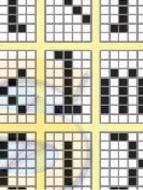
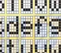
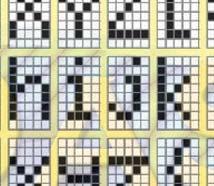
Οδηγώντας μια οθόνη υγρών κρυστάλλων Liquid Crystal Display
 Οδηγώντας μια οθόνη υγρών κρυστάλλων Liquid Crystal Display Σχηματικό Διάγραμμα μιας Οθόνης Υγρών Κρυστάλλων To Lcd εσωτερικά έχει έναν controller που είναι υπεύθυνος για την επεξεργασία τον δεδομένων
Τέτοιες λειτουργίες γίνονται διαμέσου του
 Για κάθε εντολή υπάρχουν δυο βήματα που πρέπει να γίνουν: Προσκόμιση της εντολής (fetch) από τη θέση που δείχνει ο PC Ανάγνωση των περιεχομένων ενός ή δύο καταχωρητών Τέτοιες λειτουργίες γίνονται διαμέσου
Instruction Execution Times
 1 C Execution Times InThisAppendix... Introduction DL330 Execution Times DL330P Execution Times DL340 Execution Times C-2 Execution Times Introduction Data Registers This appendix contains several tables
ΚΥΠΡΙΑΚΗ ΕΤΑΙΡΕΙΑ ΠΛΗΡΟΦΟΡΙΚΗΣ CYPRUS COMPUTER SOCIETY ΠΑΓΚΥΠΡΙΟΣ ΜΑΘΗΤΙΚΟΣ ΔΙΑΓΩΝΙΣΜΟΣ ΠΛΗΡΟΦΟΡΙΚΗΣ 19/5/2007
 Οδηγίες: Να απαντηθούν όλες οι ερωτήσεις. Αν κάπου κάνετε κάποιες υποθέσεις να αναφερθούν στη σχετική ερώτηση. Όλα τα αρχεία που αναφέρονται στα προβλήματα βρίσκονται στον ίδιο φάκελο με το εκτελέσιμο
Data sheet Thick Film Chip Resistor 5% - RS Series 0201/0402/0603/0805/1206
 Data sheet Thick Film Chip Resistor 5% - RS Series 0201/0402/0603/0805/1206 Scope -This specification applies to all sizes of rectangular-type fixed chip resistors with Ruthenium-base as material. Features
LR Series Metal Alloy Low-Resistance Resistor
 LR Series Metal Alloy LowResistance Resistor This specification is applicable to lead free, halogen free of RoHS directive for metal alloy lowresistance resistor. The product is for general purpose. The
LR(-A) Series Metal Alloy Low-Resistance Resistor
 Series Metal Alloy Low-Resistance Resistor") LR(A) Series Metal Alloy LowResistance Resistor This specification is applicable to lead free, halogen free of RoHS directive for metal alloy lowresistance resistor. The product is for general purpose.
LR(A) Series Metal Alloy LowResistance Resistor This specification is applicable to lead free, halogen free of RoHS directive for metal alloy lowresistance resistor. The product is for general purpose.
AT Surface Mount Package SOT-363 (SC-70) I I Y. Pin Connections B 1 C 1 E 1 E 2 C 2 B , 7:56 PM
 I I Y. Pin Connections B 1 C 1 E 1 E 2 C 2 B , 7:56 PM") AT-3263 Surface Mount Package SOT-363 (SC-7) I I Y Pin Connections B 1 C 1 E 1 E 2 C 2 B 2 Page 1 21.4., 7:6 PM Absolute Maximum Ratings [1] Absolute Thermal Resistance [2] : Symbol Parameter Units Maximum
AT-3263 Surface Mount Package SOT-363 (SC-7) I I Y Pin Connections B 1 C 1 E 1 E 2 C 2 B 2 Page 1 21.4., 7:6 PM Absolute Maximum Ratings [1] Absolute Thermal Resistance [2] : Symbol Parameter Units Maximum
Multilayer Ceramic Chip Capacitors
 FEATURES X7R, X6S, X5R AND Y5V DIELECTRICS HIGH CAPACITANCE DENSITY ULTRA LOW ESR & ESL EXCELLENT MECHANICAL STRENGTH NICKEL BARRIER TERMINATIONS RoHS COMPLIANT SAC SOLDER COMPATIBLE* PART NUMBER SYSTEM
Multilayer Ceramic Chip Capacitors
 FEATURES X7R, X6S, X5R AND Y5V DIELECTRICS HIGH CAPACITANCE DENSITY ULTRA LOW ESR & ESL EXCELLENT MECHANICAL STRENGTH NICKEL BARRIER TERMINATIONS RoHS COMPLIANT SAC SOLDER COMPATIBLE* Temperature Coefficient
VGS=-8V. RG=15ohm. Item Symbol Condition Limit Unit. VDS=50V, IDS1=0.9mA VDS=50V, IDS2=7.2mA
 FEATURES 2stage GaN in Plastic Package HAST Compliant GaN Technology Operable with both 28 and 50 CW Output Power: 10W @ 28, 20W @ 50 Suitable for Broadband Applications from DC to 3GHz SGFCF2002SD Plastic
CSR series. Thick Film Chip Resistor Current Sensing Type FEATURE PART NUMBERING SYSTEM ELECTRICAL CHARACTERISTICS
 FEATURE Operating Temperature: -55 ~ +155 C 3 Watts power rating in 1 Watt size, 1225 package High purity alumina substrate for high power dissipation Long side terminations with higher power rating PART
No Item Code Description Series Reference (1) Meritek Series CRA Thick Film Chip Resistor AEC-Q200 Qualified Type
 Meritek Series CRA Thick Film Chip Resistor AEC-Q200 Qualified Type") Qualified FEATURE Excellent Mechanical Strength and Electrical Stability Ideal for Pick and Place Machinery Stable High Frequency Characteristics Miniature, High Board Density Equivalent Specification
Qualified FEATURE Excellent Mechanical Strength and Electrical Stability Ideal for Pick and Place Machinery Stable High Frequency Characteristics Miniature, High Board Density Equivalent Specification
IDPV-25 series. 25W PWM Output LED Driver. File Name:IDPV-25-SPEC S&E
 5W PWM Output LED Driver IDPV5 series S&E ~ A File Name:IDPV5SPEC 0805 5W PWM Output LED Driver IDPV5 series SPECIFICATION MODEL IDPV5 IDPV5 4 IDPV5 6 IDPV5 48 IDPV5 60 DC VOLTAGE V 4V 6V 48V 60V CONSTANT
Transient Voltage Suppression Diodes: 1.5KE Series Axial Leaded Type 1500 W
 Features 1. Reliable low cost construction utilizing molded plastic technique 2. Both bi-directional and uni-directional devices are available 3. Fast response time 4. Excellent clamping capacity 5. 1500
516(5,(6. LOW NOISE 150mA LDO REGULATOR
 LOW NOISE ma LDO REGULATOR 6(,(6 NO. EA-7-4 OUTLINE 7KH6HULHVDUH&6EDVHGYROWDJHUHJXODWRU,&VZLWKKLJKRXWSXWYROWDJHDFFXUDF\H[WUHPHO\ORZVXS SO\FXUUHQWORZUHVLVWDQFHDQGKLJKLSSOHHMHFWLRQ(DFK RI WKHVH YROWDJH UHJXODWRU,&V
MAX-QUALITY ELECTRIC CO; LTD Thin Film Precision Chip Resistors. Data Sheet
 Data Sheet Customer: Product: Size: Current Sensing Chip Resistor CS Series 0201/0402/0603/0805/1206/1010/2010/2512 1225/3720/7520 Issued Date: Edition : 12-Nov-10 REV.C5 Current Sensing Chip Resistor
B37631 K K 0 60
 Multilayer Ceramic acitors High; X5R and X7R Chip Ordering code system B37631 K 7 5 K 6 Packaging 6 ^ cardboard tape, 18-mm reel 62 ^ blister tape, 18-mm reel Internal coding acitance tolerance K ^ ± %
Surface Mount Aluminum Electrolytic Capacitors
 FEATURES CYLINDRICAL V-CHIP CONSTRUCTION LOW COST, GENERAL PURPOSE, 2000 HOURS AT 85 O C NEW EXPANDED CV RANGE (up to 6800µF) ANTI-SOLVENT (2 MINUTES) DESIGNED FOR AUTOMATIC MOUNTING AND REFLOW SOLDERING
NPI Unshielded Power Inductors
 FEATURES NON-SHIELDED MAGNETIC CIRCUIT DESIGN SMALL SIZE WITH CURRENT RATINGS TO 16.5 AMPS SURFACE MOUNTABLE CONSTRUCTION TAKES UP LESS PCB REAL ESTATE AND SAVES MORE POWER TAPED AND REELED FOR AUTOMATIC
UNIVERSITY OF CALIFORNIA. EECS 150 Fall ) You are implementing an 4:1 Multiplexer that has the following specifications:
 You are implementing an 4:1 Multiplexer that has the following specifications:") UNIVERSITY OF CALIFORNIA Department of Electrical Engineering and Computer Sciences EECS 150 Fall 2001 Prof. Subramanian Midterm II 1) You are implementing an 4:1 Multiplexer that has the following specifications:
UNIVERSITY OF CALIFORNIA Department of Electrical Engineering and Computer Sciences EECS 150 Fall 2001 Prof. Subramanian Midterm II 1) You are implementing an 4:1 Multiplexer that has the following specifications:
CYTA Cloud Server Set Up Instructions
 CYTA Cloud Server Set Up Instructions ΕΛΛΗΝΙΚΑ ENGLISH Initial Set-up Cloud Server To proceed with the initial setup of your Cloud Server first login to the Cyta CloudMarketPlace on https://cloudmarketplace.cyta.com.cy
Second Order RLC Filters
 ECEN 60 Circuits/Electronics Spring 007-0-07 P. Mathys Second Order RLC Filters RLC Lowpass Filter A passive RLC lowpass filter (LPF) circuit is shown in the following schematic. R L C v O (t) Using phasor
Gearmotor Data. SERIES GM9000: We have the GM9434H187-R1
 SERIES GM9: We have the GM9434H187-R1 Gearmotor Data Item Parameter Symbol Units 5.9:1 11.5:1 19.7:1 38.3:1 65.5:1 127.8:1 218.4:1 425.9:1 728.1:1 1419.8:1 2426.9:1 4732.5:1 1 Max. Load Standard Gears
Set GPIB Address...5 Reset to startup state...5 Reboot calibrator...5 Reset to starting state...5 Identification String...5
 Table of Contents 3000A Series Remote Commands - Introduction...3 Symbols...3 Response codes...3 3000A Series Commands...4 Transmit Reading...4 Set Output, autorange...4 Set range...4 Select AC Voltage
Surface Mount Multilayer Chip Capacitors for Commodity Solutions
 Surface Mount Multilayer Chip Capacitors for Commodity Solutions Below tables are test procedures and requirements unless specified in detail datasheet. 1) Visual and mechanical 2) Capacitance 3) Q/DF
NEC Silicon RFIC Amplifiers Low Power, Wideband & SiGe/SiGeC
 NEC Silicon RFIC Amplifiers Low Power, Wideband & SiGe/SiGeC Low Power Amplifiers ELECTRICAL CHARACTERISTICS (TA = 25 C) Range VCC ICC NF Gain RLIN RLOUT PdB ISOL @ 3dB (V) (ma) (dbm) Part down Package
DRA-60 series LPS. 60W Single Output Switching Power Supply. File Name:DRA-60-SPEC Sicherheit ID
 PS Bauartgepruft Sicherheit egelma ge od o s be wac g www. tuv.com ID 2000000000 SPECIFICATION MODE DRA-60-12 DRA-60-24 DC VOTAGE 12V 24V CONSTANT CURRENT REGION 3 ~ 12V 3 ~ 24V RATED CURRENT 5A 2.5A CURRENT
38BXCS STANDARD RACK MODEL. DCS Input/Output Relay Card Series MODEL & SUFFIX CODE SELECTION 38BXCS INSTALLATION ORDERING INFORMATION RELATED PRODUCTS
 DCS Input/Output Relay Card Series STANDARD RACK MODEL 38BXCS MODEL & SUFFIX CODE SELECTION 38BXCS MODEL CONNECTOR Y1 :Yokogawa KS2 cable use Y2 :Yokogawa KS9 cable use Y6 :Yokogawa FA-M3/F3XD32-3N use
Capacitors - Capacitance, Charge and Potential Difference
 Capacitors - Capacitance, Charge and Potential Difference Capacitors store electric charge. This ability to store electric charge is known as capacitance. A simple capacitor consists of 2 parallel metal
MAX4147ESD PART 14 SO TOP VIEW. Maxim Integrated Products 1 MAX4147 EVALUATION KIT AVAILABLE ; Rev 1; 11/96 V CC V EE OUT+ IN+ R t SENSE IN-
 -; Rev ; / EVALUATION KIT AVAILABLE µ µ PART ESD TEMP. RANGE - C to +5 C PPACKAGE SO TOP VIEW V EE V CC SENSE+ SENSE- R t R t R t R t MAX SENSE OUT SENSE+ SENSE- N.C. SHDN N.C. 3 5 R f R G R f 3 VDSL TRANSFORMER
CSK series. Current Sensing Chip Resistor. Features. Applications. Construction FAITHFUL LINK
 CSK series Current Sensing Chip Resistor Features» 3 Watts power rating in 1 Watt size, 1225 Package» Low TCR of ±100 PPM/ C» Resistance values from 1m to 1 ohm» High purity alumina substrate for high
Ceramic PTC Thermistor Overload Protection
 FEATURES compliant CPTD type are bare disc type CPTL type are leaded Low, medium and high voltage ratings Low resistance; Small size No need to reset supply after overload No noise generated Stable over
60W AC-DC High Reliability Slim Wall-mounted Adaptor. SGA60E series. File Name:SGA60E-SPEC
 AC-DC High Reliability Slim Wall-mounted Adaptor SGA60E series Ⅵ Ⅴ Ⅱ Ⅱ { ψ. ψ File Name:SGA60E-SPEC 2015-09-15 AC-DC High Reliability Slim Wall-mounted Adaptor SGA60E series SPECIFICATION ORDER NO. SGA60E05-P1J
PTC FUNCTION for Delta C2000 and CP2000
 FUNCTION for Delta C2000 and CP2000 CONTENTS: GENERAL... 2. for motor temperature protection... 2.2 Standards... 2.3 Motor layout... 2.4 characteristic... 2.4. Definitions... 3.4.2 curve... 3.4.3 switching
Current Sensing Chip Resistor SMDL Series Size: 0201/0402/0603/0805/1206/1010/2010/2512/1225/3720/7520. official distributor of
 Product: Current Sensing Chip Resistor SMDL Series Size: 0201/0402/0603/0805/1206/1010/2010/2512/1225/3720/7520 official distributor of Current Sensing Chip Resistor (SMDL Series) 1. Features -3 Watts
SMD Power Inductor-VLH
 SMD Power Inductor-VH Dimensions Unit: mm Type A B C E F H I J 252010 2.5±0.2 2.0±0.2 1.0max. 0.4±0.2 1.0min. 2.1 0.90 0.8 252012 2.5±0.2 2.0±0.2 1.2max. 0.4±0.2 1.0min. 2.1 0.90 0.8 321618C 3.2±0.3 1.6±0.2
Polymer PTC Resettable Fuse:KMC Series
 Features 1. RoHS compliant 2. EIA size:1206~1812 3. Hold current ratings from 0.05 to 3A 4. Voltage ratings from 6V computer and electronic applications to 60V 5. Small footprint 6. Fast time to trip 7.
MCB and MHC Series Chip Ferrite Bead for Automotive Applications Qualified based on AEC-Q200
 RoHS MC and MHC Series Chip Ferrite ead for Automotive Applications Qualified based on AEC-Q200 Explanation of Part Number MC 1608 W 12 1 H P - 1 2 3 4 5 6 7 8 9 1. Series Name 2. Size Code: the first
AKC Spectrum Analyzer User s Manual.
 AKC-1291 Spectrum Analyzer User s Manual u ano un ao Prohibiting to removal the cover e m Keep the power insert clean RF in/output rating oae o n DC Power nt Restore this instrument 1. Introduction 2.
Multilayer Chip Inductor
 Features -Monolithic structure for high reliability -High self-resonant frequency -Excellent solderability and high heat resistance Construction Applications -RF circuit in telecommunication and other
RoHS 555 Pb Chip Ferrite Inductor (MFI Series) Engineering Spec.
 Engineering Spec.") RoHS 555 Pb Chip Ferrite Inductor (MFI Series) Engineering Spec. PRODUCT DETAIL Electrical Characteristics μh L (Min) Q MHz (Min) SRF Ω DCR IDC ma TEST FREQ: MHz TEST LEVEL: 100 mv Test Instruments HP4291
RoHS 555 Pb Chip Ferrite Inductor (MFI Series) Engineering Spec. PRODUCT DETAIL Electrical Characteristics μh L (Min) Q MHz (Min) SRF Ω DCR IDC ma TEST FREQ: MHz TEST LEVEL: 100 mv Test Instruments HP4291
Polymer PTC Resettable Fuse: KMC Series
 Features 1. RoHS & Halogen-Free (HF) compliant 2. IA size: 0603, 0805, 1206, 1812 3. Hold current ratings from 0.05 to 3A 4. Voltage ratings from 6V computer and electronic applications to 60V 5. Small
Input Ranges : 9-75 VDC
 D Series, 10- Input Ranges : 9-75 VDC : Single 3.3V - 24V Bipolar ±5.0V, ±12V, ±15V Dual +5.0V / Triple +5.0V / ±12V +5.0V / ±15V Power: 6.6 to 15 W The D series DC-DC converters feature high power density,
Potential Dividers. 46 minutes. 46 marks. Page 1 of 11
 Potential Dividers 46 minutes 46 marks Page 1 of 11 Q1. In the circuit shown in the figure below, the battery, of negligible internal resistance, has an emf of 30 V. The pd across the lamp is 6.0 V and
ΤΜΗΜΑ ΜΗΧΑΝΙΚΩΝ ΠΛΗΡΟΦΟΡΙΚΗΣ ΚΑΙ ΥΠΟΛΟΓΙΣΤΩΝ ΕΡΓΑΣΤΗΡΙΟ: ΜΙΚΡΟΕΛΕΓΚΤΕΣ
 ΤΜΗΜΑ ΜΗΧΑΝΙΚΩΝ ΠΛΗΡΟΦΟΡΙΚΗΣ ΚΑΙ ΥΠΟΛΟΓΙΣΤΩΝ ΕΡΓΑΣΤΗΡΙΟ: ΜΙΚΡΟΕΛΕΓΚΤΕΣ Ι. Έλληνας Δεκέμβριος 2018 Άσκηση 1 Να συνδεθεί ο Arduino Uno με το LED matrix 8X8 μέσω SPI. Να γραφτεί πρόγραμμα το οποίο θα δημιουργεί
Current Sensing Chip Resistor
 Features -3 atts power rating in 1 att size, 1225 package -Low CR of ±100 PPM/ C -Resistance values from 1m to 1 ohm -High purity alumina substrate for high power dissipation -Long side terminations with
High Performance Voltage Controlled Amplifiers Typical and Guaranteed Specifications 50 Ω System
 High Performance Voltage Controlled Amplifiers Typical and Guaranteed Specifications 50 Ω System Typical and guaranteed specifications vary versus frequency; see detailed data sheets for specification
SMD Power Inductor-VLH
 SMD Power Inductor-VH PAD AYOUT Dimensions Unit: mm Type A B C E F H I J 252010 2.5±0.2 2.0±0.2 1.0max. 0.4±0.2 1.0min. 2.1 0.90 0.8 252012 2.5±0.2 2.0±0.2 1.2max. 0.4±0.2 1.0min. 2.1 0.90 0.8 252510 2.5±0.2
Monolithic Crystal Filters (M.C.F.)
") Monolithic Crystal Filters (M.C.F.) MCF (MONOLITHIC CRYSTAL FILTER) features high quality quartz resonators such as sharp cutoff characteristics, low loss, good inter-modulation and high stability over
Monolithic Crystal Filters (M.C.F.) MCF (MONOLITHIC CRYSTAL FILTER) features high quality quartz resonators such as sharp cutoff characteristics, low loss, good inter-modulation and high stability over
DRA-40 series LPS. 40W Single Output Switching Power Supply. File Name:DRA-40-SPEC Sicherheit ID
 PS Bauartgepruft Sicherheit egelma ge od o s be wac g www. tuv.com ID 2000000000 SPECIFICATION MODE OUTPUT WORKING TEMP. WORKING HUMIDITY ENVIRONMENT STORAGE TEMP., HUMIDITY TEMP. COEFFICIENT VIBRATION
NTC Thermistor:TTC3 Series
 Features. RoHS compliant 2. Halogen-Free(HF) series are available 3. Body size: Ф3mm 4. Radial lead resin coated 5. Operating temperature range: -40 ~+25 6. Wide resistance range 7. Cost effective 8. Agency
SMD Power Inductor. - SPRH127 Series. Marking. 1 Marking Outline: 1 Appearance and dimensions (mm)
") Marking Outline: Low DCR, high rated current. Magnetic shielded structure Lead free product, RoHS compliant. RoHS Carrier tape packing, suitable for SMT process. SMT Widely used in buck converter, laptop,
Marking Outline: Low DCR, high rated current. Magnetic shielded structure Lead free product, RoHS compliant. RoHS Carrier tape packing, suitable for SMT process. SMT Widely used in buck converter, laptop,
NPN SILICON OSCILLATOR AND MIXER TRANSISTOR
 FEATURES NPN SILICON OSCILLATOR AND MIXER TRANSISTOR LOW COST HIGH GAIN BANDWIDTH PRODUCT: ft = MHz TYP LOW COLLECTOR TO BASE TIME CONSTANT: CC r b'b = 5 ps TYP LOW FEEDBACK CAPACITANCE: CRE=.55 pf TYP
Metal Oxide Leaded Film Resistor
 SURFACE TEMP. RISE ( ) Power Ratio(%) MOF0623, 0932, 1145, 1550, 1765, 2485 MOF Series Features -Excellent Long-Time stability -High surge / overload capability -Wide resistance range : 0.1Ω~10MΩ -Controlled
Ceramic PTC Thermistor Overload Protection
 FEATURES compliant CPTD type are bare disc type CPTL type are leaded Low, medium and high voltage ratings Low resistance; Small size No need to reset supply after overload No noise generated Stable over
Siemens AG Rated current 1FK7 Compact synchronous motor Natural cooling. I rated 7.0 (15.4) 11.5 (25.4) (2.9) 3.3 (4.4)
 11.5 (25.4) (2.9) 3.3 (4.4)") Synchronous motors Siemens 2009 FK7 Compact motors Nural cooling Selection and ordering da Red speed Shaft height n red S P red ΔT=00 K rpm kw (P) Red power Stic torque M 0 ΔT=00 K Red torque ) M red ΔT=00
Synchronous motors Siemens 2009 FK7 Compact motors Nural cooling Selection and ordering da Red speed Shaft height n red S P red ΔT=00 K rpm kw (P) Red power Stic torque M 0 ΔT=00 K Red torque ) M red ΔT=00
SMC SERIES Subminiature Coaxial Connectors
 SERIES Subminiature Coaxial Connectors FEATURES Subminiature coaxial connectors with 50 Ω impedance for applications up to 10 GHz. (screw on mechanism)fulfills the subminiature coaxial connector requirement
Anti-Corrosive Thin Film Precision Chip Resistor (PR Series)
") (PR Series) Features -Long term life stability and demonstrated the Anti Corrosion claims -Special passivated NiCr film for Anti-Acid and Anti-Damp -Tight tolerance down to ±0.1% -Extremely low TCR down
(PR Series) Features -Long term life stability and demonstrated the Anti Corrosion claims -Special passivated NiCr film for Anti-Acid and Anti-Damp -Tight tolerance down to ±0.1% -Extremely low TCR down
INPAQ Global RF/Component Solutions
 MCB & MHC W Series Specification Product Name Series Multilayer Chip Ferrite Bead MCB & MHC W Series Size EIAJ 1005/1608/2012/3216/4516 MCB and MHC Series Chip Ferrite Bead for Automotive Applications
Aluminum Electrolytic Capacitors
 Aluminum Electrolytic Capacitors Snap-In, Mini., 105 C, High Ripple APS TS-NH ECE-S (G) Series: TS-NH Features Long life: 105 C 2,000 hours; high ripple current handling ability Wide CV value range (47
SMD Wire Wound Ferrite Chip Inductors - LS Series. LS Series. Product Identification. Shape and Dimensions / Recommended Pattern LS0402/0603/0805/1008
 SMD Wire Wound Ferrite Chip Inductors - LS Series LS Series LS Series is the newest in open type ferrite wire wound chip inductors. The wire wound ferrite construction supports higher SRF, lower DCR and
ΑΥΤΟΜΑΤΟΠΟΙΗΣΗ ΜΟΝΑΔΑΣ ΘΡΑΥΣΤΗΡΑ ΜΕ ΧΡΗΣΗ P.L.C. AUTOMATION OF A CRUSHER MODULE USING P.L.C.
 ΤΕΧΝΟΛΟΓΙΚΟ ΕΚΠΑΙΔΕΥΤΙΚΟ ΙΔΡΥΜΑ ΑΝ. ΜΑΚΕΔΟΝΙΑΣ ΚΑΙ ΘΡΑΚΗΣ ΣΧΟΛΗ ΤΕΧΝΟΛΟΓΙΚΩΝ ΕΦΑΡΜΟΓΩΝ ΤΜΗΜΑ ΗΛΕΚΤΡΟΛΟΓΩΝ ΜΗΧΑΝΙΚΩΝ Τ.Ε ΠΤΥΧΙΑΚΗ ΕΡΓΑΣΙΑ ΑΥΤΟΜΑΤΟΠΟΙΗΣΗ ΜΟΝΑΔΑΣ ΘΡΑΥΣΤΗΡΑ ΜΕ ΧΡΗΣΗ P.L.C. AUTOMATION OF A
Metal Oxide Leaded Film Resistor
 Features -Excellent Long-Time stability -High surge / overload capability -Wide resistance range : 0.1Ω~22MΩ -Controlled temperature coefficient -Resistance standard tolerance: ±5% (consult factory for
Πρόβλημα 1: Αναζήτηση Ελάχιστης/Μέγιστης Τιμής
 Πρόβλημα 1: Αναζήτηση Ελάχιστης/Μέγιστης Τιμής Να γραφεί πρόγραμμα το οποίο δέχεται ως είσοδο μια ακολουθία S από n (n 40) ακέραιους αριθμούς και επιστρέφει ως έξοδο δύο ακολουθίες από θετικούς ακέραιους
SMC SERIES Subminiature Coaxial Connectors
 SERIES Subminiature Coaxial Connectors FEATURES Subminiature coaxial connectors with 50 Ω impedance for applications up to 10 GHz. (screw on mechanism)fulfills the subminiature coaxial connector requirement
Homework 8 Model Solution Section
 MATH 004 Homework Solution Homework 8 Model Solution Section 14.5 14.6. 14.5. Use the Chain Rule to find dz where z cosx + 4y), x 5t 4, y 1 t. dz dx + dy y sinx + 4y)0t + 4) sinx + 4y) 1t ) 0t + 4t ) sinx
CMOS Technology for Computer Architects
 CMOS Technology for Computer Architects Iakovos Mavroidis Giorgos Passas Manolis Katevenis Lecture 13: On chip SRAM Technology FORTH ICS / EURECCA & UoC GREECE ABC A A E F A BCDAECF A AB C DE ABCDAECF
FEATURES APPLICATION PRODUCT T IDENTIFICATION PRODUCT T DIMENSION MAG.LAYERS
 FEATURES RoHS compliant. Super low resistance, ultra high current rating. High performance (I sat) realized by metal dust core. Frequency Range: up to 1MHz. APPLICATION PDA, notebook, desktop, and server
ΚΥΠΡΙΑΚΗ ΕΤΑΙΡΕΙΑ ΠΛΗΡΟΦΟΡΙΚΗΣ CYPRUS COMPUTER SOCIETY ΠΑΓΚΥΠΡΙΟΣ ΜΑΘΗΤΙΚΟΣ ΔΙΑΓΩΝΙΣΜΟΣ ΠΛΗΡΟΦΟΡΙΚΗΣ 24/3/2007
 Οδηγίες: Να απαντηθούν όλες οι ερωτήσεις. Όλοι οι αριθμοί που αναφέρονται σε όλα τα ερωτήματα μικρότεροι του 10000 εκτός αν ορίζεται διαφορετικά στη διατύπωση του προβλήματος. Αν κάπου κάνετε κάποιες υποθέσεις
Aluminum Electrolytic Capacitors (Large Can Type)
") Aluminum Electrolytic Capacitors (Large Can Type) Snap-In, 85 C TS-U ECE-S (U) Series: TS-U Features General purpose Wide CV value range (33 ~ 47,000 µf/16 4V) Various case sizes Top vent construction
Aluminum Electrolytic Capacitors (Large Can Type) Snap-In, 85 C TS-U ECE-S (U) Series: TS-U Features General purpose Wide CV value range (33 ~ 47,000 µf/16 4V) Various case sizes Top vent construction
No item Digit Description Series Reference (1) Meritek Series SI Signal Inductor LI: Leaded Inductor PI: Power Inductor
 Meritek Series SI Signal Inductor LI: Leaded Inductor PI: Power Inductor") PART NUMBERING SYSTEM SI F 0805 K 780 F (1) (2) (3) (4) (5) (6) No item Digit Description Series Reference (1) Meritek Series SI Signal Inductor LI: Leaded Inductor PI: Power Inductor (2) Type F Ferrite
PART NUMBERING SYSTEM SI F 0805 K 780 F (1) (2) (3) (4) (5) (6) No item Digit Description Series Reference (1) Meritek Series SI Signal Inductor LI: Leaded Inductor PI: Power Inductor (2) Type F Ferrite
Power Inductor LVS Series
 RoHS Compliant Halogen Free REACH Compliant Part Numbering LVS 6645 L - 1R M - AU Series Name Dimensions Code Inductance Internal Code (mm) (uh) Tolerance 4412 4.x4.x1.2 L Low DCR R47.47 M ±% 4418 4.x4.x1.8
k A = [k, k]( )[a 1, a 2 ] = [ka 1,ka 2 ] 4For the division of two intervals of confidence in R +
[a 1, a 2 ] = [ka 1,ka 2 ] 4For the division of two intervals of confidence in R +](/thumbs/73/69566903.jpg "k A = [k, k]( )[a 1, a 2 ] = [ka 1,ka 2 ] 4For the division of two intervals of confidence in R +") Chapter 3. Fuzzy Arithmetic 3- Fuzzy arithmetic: ~Addition(+) and subtraction (-): Let A = [a and B = [b, b in R If x [a and y [b, b than x+y [a +b +b Symbolically,we write A(+)B = [a (+)[b, b = [a +b
Chapter 3. Fuzzy Arithmetic 3- Fuzzy arithmetic: ~Addition(+) and subtraction (-): Let A = [a and B = [b, b in R If x [a and y [b, b than x+y [a +b +b Symbolically,we write A(+)B = [a (+)[b, b = [a +b