Selection guide Discretes, Logic and MOSFETs
|
|
|
- Πολύμνια Καλογιάννης
- 7 χρόνια πριν
- Προβολές:
Transcript

1 Selection guide Discretes, Logic and MOSFETs
2 Introduction Welcome to the 2018 edition of the Nexperia Selection Guide. Here we present all our Discrete, Logic and MOSFET devices in one single document to give you a complete overview of our portfolio. We hope that makes it even easier for you to find the right product for your design. Our extensive portfolio offers a wide range of general purpose devices and those that meet the stringent standards set by the automotive industry. They are housed in some of the most advanced, industry-leading small packages that combine power and thermal efficiency with best-in-class quality levels. Alongside quality and efficiency, Nexperia customers value reliability and a consistent supply they can trust. We produce consistently reliable semiconductor components at high volume (85 billion annually) and we work at every step to safeguard the long-term availability of our manufacturing processes and products, to ensure secure supply for all our customers. We have a long history and broad experience. That ensures we can support you with the dedicated inhouse technical support you need from simplifying selection via quick-reference material to simple-touse design tools and application insights. All to help drive up efficiency in your designs. All the functionality you need in one spot Just like on our website, you will find the selection guide is split into our five key product areas. There is also a dedicated section on packages, highlighting the latest package innovations and packing options. Bipolar transistors Resistor-equipped, low V CEsat and small-signal transistors Standard SMD, leadless and clip-bond packages Diodes Broad choice of Zener, Schottky and switching diodes Ultra-small, low-profile surface-mount package options ESD protection, filtering and signal conditioning Extensive range of protection in ultra-small form factors Optimized for signal integrity, robustness and system protection MOSFETs Low R DSon devices from < 20 V to > 200 V True power packages with solid wireless-clip for smart efficiency Logic Comprehensive portfolio operating from 0.7 V to 15.0 V Unrivalled package innovation and lowest power logic solutions Packages The next generation of packaging for volume production Package cross-reference and packing options As an innovative company we are continually adding to our product portfolio, so to discover all our latest product information you should visit our website
3 Our commitment: quality and reliability AEC- Q100/Q101 AEC-Q100/Q101 qualified Go for quality We qualify our products according to the automotive AEC-Q100/Q101 standard and even exceed it s requirements, for instance when doing extended lifetime testing. All our processes and manufacturing plants are subject to regular international and internal audits, including the following: ISO9001 ISO/TS for automotive sites ISO14001 OHSAS18001 Design for excellence Zero defect Nexperia s Design for Excellence (DfX) program ensures that each new development builds on past learning and that best practices are always employed. The result is continual product improvement. Zero defect is our goal. To ensure continuous improvement failure analysis and the determination to find root causes is performed at all stages of development and production by adoption of quality-analysis tools and methods (e.g. Six-Sigma, Safe-Launch). Rigorous attention to detail and commitment to quality have yielded a very low product failure rate of a single-digit part per billion (ppb).
4
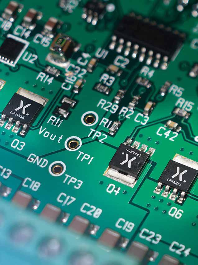
5 Bipolar transistors Selection guide Discretes, Logic and MOSFETs Diodes 1 2 ESD protection, TVS, filtering and signal conditioning 3 MOSFETs 4 Logic 5 Packages 6
6 New products... 8 Bipolar transistors... 8 Diodes... 9 ESD protection, TVS, filtering and signal conditioning... 9 MOSFETs Logic Bipolar transistors 13 General purpose bipolar transistors...14 Transistors single NPN Transistors single PNP High performance transistors (superior power dissipation) Transistors double Switching transistors single Switching transistors double Medium power transistors Medium power transistors high performance (175 C capable) High performance transistors (175 C capable & superior power dissipation) High voltage transistors LED driver Constant current source Darlington transistors Schmitt triggers Low noise transistors Matched pair transistors - part Matched pair transistors - part MOSFET driver Medium frequency transistors Low V CEsat (BISS) transistors...22 Low V CEsat (BISS) transistors single NPN up to 2000 mw Low V CEsat (BISS) transistors single NPN up to 750 mw Low V CEsat (BISS) transistors single PNP up to 2000 mw Low V CEsat (BISS) transistors single PNP up to 750 mw Low V CEsat (BISS) transistors double Low V CEsat (BISS) transistors load switches Low V CEsat (BISS) high voltage transistors Low V CEsat (BISS) RETs Low V CEsat (BISS) transistors PNP - N-channel MOSFET combination Low V CEsat (BISS) power transistors single Low V CEsat (BISS) power transistors double Resistor equipped transistors (RETs)...30 RETs 100 ma single - part RETs 100 ma single - part RETs 100 ma double RETs 500mA single / double terminal adjustable shunt regulators...32 Diodes 35 Zener diodes...36 General purpose Zener diodes Zener diodes specifications Switching diodes...38 General purpose, high speed switching diodes <= 90V General purpose, high speed switching diodes 100V General purpose, switching diodes >= 100V Controlled avalanche switching diodes Low leakage current switching diodes PN rectifiers PN rectifiers...41 PN rectifiers - Automotive qualified Nomenclature pn-rectifier consumer grade types Nomenclature pn-rectifier automotive grade types Schottky rectifiers...42 General purpose schottky diodes <= 250 ma Low capacitance schottky diodes Medium power low VF schottky rectifiers single >= 200 ma - leadless DSN / DFN packages Medium power low VF schottky rectifiers single >= 200 ma Medium power low VF schottky rectifiers single >= 200 ma - leaded packages Medium power low VF schottky rectifiers dual >= 200 ma Nomenclatures...49 ESD protection, TVS, filtering and signal conditioning 51 Low capacitance ESD protection for high-speed interfaces...52 Low capacitance ESD protection for high-speed interfaces TrEOS protection devices General ESD protection devices...58 General purpose ESD protection devices Application-specific ESD solutions...60 Audio interface protection Automotive high-speed network protection Automotive in-vehicle network bus line protection Battery and charger port protection HDMI and display port protection Antenna protection (NFC, WiFi, ) USB and SATA protection EMI solutions with integrated protection...64 Common mode filter for USB Common mode filter for USB 3.x Common mode filter for HDMI and MIPI HDMI signal conditioning LCD and camera RC filter with integrated protection Memory and SIM card filter with integrated protection.. 66 USB 3.x and esata protection and filtering for high-speed and super-speed lines Transient voltage surge suppressor (TVS)...67 TVS diodes for mobile applications TVS diodes, 24 W/40 W (automotive) TVS diodes, 400 W TVS diodes, 600W Nomenclatures...70 MOSFETs 73 Automotive MOSFETs...74 Automotive grade MOSFETs nomenclature N-channel 30V automotive power MOSFETs N-channel 40V automotive power MOSFETs N-channel 55V-60V automotive power MOSFETs N-channel 75V-80V automotive power MOSFETs N-channel 100V automotive power MOSFETs Small-signal automotive MOSFETs Low R DS(on) Small-signal automotive MOSFETs High R DS(on) Small-signal automotive MOSFETs Dual... 84
7 Power MOSFETs...86 N-channel 25V-30V MOSFETs N-channel 40V-60V MOSFETs N-channel 75V-200V MOSFETs P-channel MOSFETs Power MOSFETs nomenclature Small-signal MOSFETs...94 Small-signal MOSFETs in DFN1006 and DFN1006B packages Small-signal MOSFETs in DFN1010D-3 single and DFN1010B-3 dual packages Small-signal low-leakage MOSFETs Small-signal MOSFETs in DFN2020MD-6 single and DFN dual packages Small-signal MOSFETs in WLCSP4 and WLCSP6 packages 97 Small-signal MOSFETs single (N-channel) Small-signal MOSFETs single (P-channel) Small-signal MOSFET Schottky combination Small-signal MOSFETs dual Small-signal MOSFETs complementary Logic 105 Automotive logic Analog switches Buffers/Inverters Buffers/Inverters Counters/Frequency dividers Bus switches Digital decoders/demultiplexers Digital multiplexers Flip-flops Flip-flops Flip-flops Gates Latches/Registered drivers Gates Level shifters/translators Multivibrators Schmitt-triggers Shift registers Shift registers Transceivers Analog switches Bus switches Buffers/Inverters Buffers/Inverters Digital decoders/demultiplexers Digital multiplexers Flip-flops Gates Gates Latches/Registered drivers Multivibrators Schmitt-triggers Level shifters/translators Buffers, Drivers, Transceivers Buffers/Inverters/Drivers Transceivers Schmitt-triggers Counters/Frequency dividers Flip-flops, Latches, Registers FIFO registers Flip-flops Latches/Registered drivers Contents Gates AND Gates Combination Gates Configurable Gates EXCLUSIVE-NOR Gates EXCLUSIVE-OR Gates NAND Gates NOR Gates OR Gates Logic voltage translators Level shifters/translators Specialty logic Digital comparators Multivibrators Parity generators-checkers Phase-locked loops Printer interfaces Switches, Multiplexers, Demultiplexers Bus Switches Decoders/Demultiplexers Digital Multiplexers Analog Switches Nomenclatures Packages 163 Package details and packing methods Package details and packing methods SMD Part Package details and packing methods SMD Part Package details and packing methods SMD Part Package details and packing methods SMD Part Package details and packing methods WLCSP Packing details glass diodes, single ended and through hole packages Package cross reference Package cross reference list Part Package cross reference list Part Package cross reference list Part Package cross reference list Part Package cross reference list Part Package cross reference matrix Part Package cross reference matrix Part Package cross reference matrix Part Competitive cross reference - Logic Packing methods Product orientation (tape and reel pack) Minimized outline drawings and reflow soldering footprint pin SMD packages pin SMD packages pin SMD packages pin SMD packages pin SMD packages pin SMD packages pin SMD packages pin SMD packages More than 8-pin SMD packages Glass diodes Single-ended and through-hole packages Index Bipolar transistors Diodes ESD protection, TVS, filtering and signal conditioning MOSFETs Logic Packages
8 New products As an innovative company we invest significantly in R&D, and continually expand our portfolio with the latest generation of technology and products. Here is a snapshot of our most recent releases, but don't forget to visit the website for the most up-to-date information - Bipolar transistors Category Device Description Page BC817K V, 500 ma NPN general-purpose transistors in SOT23 15 BC817K V, 500 ma NPN general-purpose transistors in SOT23 15 BC817K V, 500 ma NPN general-purpose transistors in SOT23 15 BC807K V, 500 ma PNP general-purpose transistors in SOT23 15 BC807K V, 500 ma PNP general-purpose transistors in SOT23 15 BC807K V, 500 ma PNP general-purpose transistors in SOT23 15 BCP56H 80 V, 1 A NPN medium power transistor in SOT BCP56-10H 80 V, 1 A NPN medium power transistor in SOT BCP56-16H 80 V, 1 A NPN medium power transistor in SOT BCP53H 80 V, 1 A PNP medium power transistors in SOT General purpose bipolar transistors BCP53-10H 80 V, 1 A PNP medium power transistors in SOT BCP53-16H 80 V, 1 A PNP medium power transistors in SOT BC817K-16H 45 V, 500 ma NPN general-purpose transistors in SOT23 17 BC817K-25H 45 V, 500 ma NPN general-purpose transistors in SOT23 17 BC817K-40H 45 V, 500 ma NPN general-purpose transistors in SOT23 17 BCM56DS NPN/NPN matched double transistors in SOT BCM53DS PNP/PNP matched double transistors in SOT BCM847QAS NPN/NPN matched double transistors in SOT BCM857QAS PNP/PNP matched double transistors in SOT PMP4501QAS NPN/NPN matched double transistors in SOT PMP5501QAS PNP/PNP matched double transistors in SOT PBSS4160X 60 V, 1 A NPN low VCEsat BISS transistor in SOT89 22 PBSS4360X 60 V, 3 A NPN low VCEsat BISS transistor in SOT89 22 PBSS5360X 60 V, 3 A PNP low VCEsat (BISS) transistor in SOT89 24 Low VCEsat (BISS) transistors PBSS5250TH 50 V, 2 A PNP low VCEsat (BISS) transistor in SOT23 25 PBSS5350TH 50 V, 3 A PNP low VCEsat (BISS) transistor in SOT23 25 PBHV9540X 400 V, 0.5 A PNP high-voltage low VCEsat (BISS) transistor in SOT89 28 PHPT61002NYCLH 100 V, 2 A NPN high power bipolar transistor in LFPAK56 29 PHPT61002PYCLH 100 V, 2 A PNP high power bipolar transistor in LFPAK56 29 PRMH11 50 V, 100 ma NPN/NPN Resistor-Equipped double Transistors (RET) in ultra-small DFN PRMD3 50 V, 100 ma NPN/PNP Resistor-Equipped double Transistors (RET) in ultra-small DFN PRMB11 50 V, 100 ma PNP/PNP Resistor-Equipped double Transistors (RET) in ultra-small DFN PRMD2 50 V, 100 ma NPN/PNP Resistor-Equipped double Transistors (RET) in ultra-small DFN PRMH2 50 V, 100 ma NPN/NPN Resistor-Equipped double Transistors (RET) in ultra-small DFN Resistor equipped transistors (RETs) PRMD12 50 V, 100 ma NPN/PNP Resistor-Equipped double Transistors (RET) in ultra-small DFN PRMH10 50 V, 100 ma NPN/NPN Resistor-Equipped double Transistors (RET) in ultra-small DFN PRMD10 50 V, 100 ma NPN/PNP Resistor-Equipped double Transistors (RET) in ultra-small DFN PRMH13 50 V, 100 ma NPN/NPN Resistor-Equipped double Transistors (RET) in ultra-small DFN PRMD13 50 V, 100 ma NPN/PNP Resistor-Equipped double Transistors (RET) in ultra-small DFN PRMH9 50 V, 100 ma NPN/NPN Resistor-Equipped double Transistors (RET) in ultra-small DFN PRMD16 50 V, 100 ma NPN/PNP Resistor-Equipped double Transistors (RET) in ultra-small DFN Nexperia selection guide 2018
9 New products Diodes Category Device Description Page Switching Diodes BAS321J General purpose diode, planar technology, encapsulated in a very small plastic SOD323F (SC-90) package 39 ES1DVR 200V, 1A Hyperfast PN Rectifier in CFP3 (low VF) 40 ES1DR 200V, 1A Hyperfast PN Rectifier in CFP3 40 ES2DVR 200V, 2A Hyperfast PN Rectifier in CFP3 (low VF) 40 PN Rectifiers ES2DR 200V, 2A Hyperfast PN Rectifier in CFP3 40 ES2DP 200V, 2A Hyperfast PN Rectifier in CFP5 40 ES3DP 200V, 3A Hyperfast PN Rectifier in CFP5 40 ES1GR 400V, 1A Hyperfast PN Rectifier in CFP3 40 PNE20030EP 200V, 3A Hyperfast PN Rectifier in CFP5 (Automotive grade) 41 PN Rectifiers - Automotive PNE20020EP 200V, 2A Hyperfast PN Rectifier in CFP5 (Automotive grade) 41 PNE20020ER 200V, 2A Hyperfast PN Rectifier in CFP3 (Automotive grade) 41 PNE20010ER 200V, 1A Hyperfast PN Rectifier in CFP3 (Automotive grade) 41 PMEG60T20ELR 60 V, 2 A low leakage current Trench MEGA Schottky barrier rectifier in CFP3 45 PMEG40T10ER 40V, 1A Trench Schottky Rectifier in CFP3 46 PMEG40T20EP 40V, 2A Trench Schottky Rectifier in CFP5 46 PMEG40T20ER 40V, 2A Trench Schottky Rectifier in CFP3 46 PMEG045T030EPD 45V, 3A Trench Schottky Rectifier in CFP15 46 Schottky rectifiers PMEG40T30EP 40V, 3A Trench Schottky Rectifier in CFP5 46 PMEG40T30ER 40V, 3A Trench Schottky Rectifier in CFP3 46 PMEG40T50EP 40V, 5A Trench Schottky Rectifier in CFP5 46 PMEG045T050EPD 45V, 5A Trench Schottky Rectifier in CFP15 46 PMEG045T100EPD 45V, 10A Trench Schottky Rectifier in CFP15 46 PMEG045T150EIPD 45V, 15A Trench Schottky Rectifier in CFP15 46 ESD protection, TVS, filtering and signal conditioning Category Device Description Page Low capacitance ESD protection for high-speed interfaces PHDMI2FR4 Very low-clamping ESD protection for HDMI 55 PHDMI2AB4 Very low capacitance ESD protection for HDMI 55 General ESD protection devices PESD3V3T1BL Ultra compact Transient Voltage Supressor in DFN Application-specific ESD solutions PESD2ETH-D ESD protection for in-vehicle ultra high-speed interfaces, in SOT457 package 61 PESD2ETH-AD ESD protection for in-vehicle ultra high-speed interfaces, in SOT457 package 61 PCMF1HDMI2S Common Mode Filter with ESD protection for HDMI PCMF2HDMI2S Common Mode Filter with ESD protection for HDMI PCMF3HDMI2S Common Mode Filter with ESD protection for HDMI PUSB3FR6 Very low-clamping ESD protection for six data lines 66 PUSB3AB6 Very low-capacitance ESD protection for six data lines 66 EMI solutions with integrated protection PUSB3F97 Very low-clamping ESD protection for USB3.2@ 10 Gbps 66 PESD3V3W1BSF Extremely low-clamping, high robustness ESD protection for USB PESD4V0W1BSF Extremely low-clamping, high robustness ESD protection for USB PESD7V0R1BSF Extremely low-capacitance ESD-protection with 7 V V_RWM 66 PESD7V0H1BSF Very low-capacitance ESD-protection with 7 V V_RWM 66 PESD7V0C1BSF Extremely low-clamping ESD-protection with 7 V V_RWM 66 PESD6V5C1USF Extremely low-clamping unidirectional ESD-protection with 6.5 V V_RWM 66 9
10 New products ESD protection, TVS, filtering and signal conditioning Category Device Description Page PTVS4V5D1BL Ultra compact Transient Voltage Supressor in ultra-small DFN MMBZ16VAL High surge current unidirectional double ESD protection diodes in SOT23 (automotive grade) 67 Transient voltage surge suppressor (TVS) MMBZ16VTAL High surge current unidirectional double ESD protection diodes in SOT23 (automotive grade) 67 PTVS20VU1UPA 300 W unidirectional Transient Voltage Suppressor (TVS) in DFN PTVS22VU1UPA 300 W unidirectional Transient Voltage Suppressor (TVS) in DFN PTVS24VU1UPA 300 W unidirectional Transient Voltage Suppressor (TVS) in DFN PTVS5V0Z1USKP Transient voltage suppressor in DSN for mobile applications 67 MOSFETs Category Device Description Page BUK7J1R4-40H N-channel 40 V, 1.4 mω standard level Q101 MOSFET in LFPAK56E 75 BUK7Y1R7-40H N-channel 40 V, 1.7 mω standard level Q101 MOSFET in LFPAK56 75 Automotive MOSFETs BUK7Y2R0-40H N-channel 40 V, 2 mω standard level Q101 MOSFET in LFPAK56 75 BUK7Y2R5-40H N-channel 40 V, 2.5 mω standard level Q101 MOSFET in LFPAK56 75 BUK7Y3R0-40H N-channel 40 V, 3 mω standard level Q101 MOSFET in LFPAK56 75 PSMN8R5-100PSF NextPower 100 V, 8.7 mω N-channel MOSFET in TO220 package 90 PSMN PSF NextPower 100 V, 18 mω N-channel MOSFET in TO220 package 90 PSMN8R5-100ESF NextPower 100 V, 8.8 mω N-channel MOSFET in I2PAK package 91 Power MOSFETs PSMN ESF NextPower 100 V, 18 mω N-channel MOSFET in I2PAK package 91 PSMN5R6-100YSF NextPower 100 V, 6 mω N-channel MOSFET in LFPAK56 package 92 PSMN6R9-100YSF NextPower 100 V, 7 mω N-channel MOSFET in LFPAK56 package 92 PSMN8R7-100YSF NextPower 100 V, 9 mω N-channel MOSFET in LFPAK56 package 92 PMCM4401UNE 20 V, N-channel Trench MOSFET in 4 bumps Wafer Level Chip-Size Package (WLCSP) 97 PMCM4402UPE 20 V, P-channel Trench MOSFET in 4 bumps Wafer Level Chip-Size Package (WLCSP) 97 PMCM6501UNE 20 V, N-channel Trench MOSFET in 6 bumps Wafer Level Chip-Size Package (WLCSP) 97 Small-signal MOSFETs PMCM6501UPE 20 V, P-channel Trench MOSFET in 6 bumps Wafer Level Chip-Size Package (WLCSP) 97 PMCM6501CUNE 20 V, N-channel Trench MOSFET in 6 bumps Wafer Level Chip-Size Package (WLCSP) 97 PMV280ENEA 100 V N-channel Trench MOSFET in SOT23 SMD package 99 PMN70EPE 30 V, P-channel Trench MOSFET in SOT457 SMD package Nexperia selection guide 2018
11 New products Logic Category Device Description Page 74CBTLV3125-Q100 Quad bus switch HC161-Q100 Presettable synchronous 4-bit binary counter; asynchronous reset 109 Automotive Logic 74LVC4T3144-Q100 4-bit dual-supply buffer/line driver; 3-state 116 HEF4528B-Q100 Dual monostable multivibrator LVC1G19-Q100 1-to-2 decoder/demultiplexer AHC9541A Octal buffer/line driver; Schmitt-trigger (3-state) AHCT07A Hex buffer with open-drain; TTL-enabled AHCT244A Octal buffer/line driver (3-state) AHCT541A Octal buffer/line driver; TTL-enabled (3-state) 130 Buffers/inverters/drivers 74LV04AT Hex inverter with TTL inputs LV05A Hex inverter; open-drain LV07AT Hex buffer with open-drain; TTL-enabled LV244A Octal buffer/line driver (3-state) LV244AT Octal buffer/line driver; TTL-enabled (3-state) LV540A Octal buffer/line driver (3-state); inverting AHCV07A Hex buffer with open-drain outputs; Schmitt-trigger AHCV244A Octal buffer/line driver; Schmitt-trigger (3-state) 130 Schmitt-triggers 74AHCV541A Octal buffer/line driver; Schmitt-trigger (3-state) LV17A Hex buffer; Schmitt-trigger AHCT17A Hex buffer; Schmitt-trigger 138 Gates 74AUP2G132 Low-power dual 2-input NAND gate; Schmitt-trigger 139 Logic voltage translators 74LVC8T595 Dual-supply 8-bit serial-in/serial-out or parallel out translating shift register (3-state) 154 Bus switches 74CB3Q3253 Dual 1-of-4 FET multiplexer/demultiplexer with charge pump CB3Q3257 Quad 1-of-2 FET multiplexer/demultiplexer with charge pump
12
13 Bipolar transistors 1 General purpose bipolar transistors...14 Transistors single NPN...14 Transistors single PNP...14 High performance transistors (superior power dissipation)...15 Transistors double...15 Switching transistors single...16 Switching transistors double...16 Medium power transistors...17 Medium power transistors high performance (175 C capable)...17 High performance transistors (175 C capable & superior power dissipation)...17 High voltage transistors...18 LED driver...18 Constant current source...18 Darlington transistors...19 Schmitt triggers...19 Low noise transistors...19 Matched pair transistors - part Matched pair transistors - part MOSFET driver...21 Medium frequency transistors...21 Low V CEsat (BISS) transistors...22 Low V CEsat (BISS) transistors single NPN up to 2000 mw...22 Low V CEsat (BISS) transistors single NPN up to 750 mw...23 Low V CEsat (BISS) transistors single PNP up to 2000 mw...24 Low V CEsat (BISS) transistors single PNP up to 750 mw...25 Low V CEsat (BISS) transistors double...26 Low V CEsat (BISS) transistors load switches...27 Low V CEsat (BISS) high voltage transistors...28 Low V CEsat (BISS) RETs...28 Low V CEsat (BISS) transistors PNP - N-channel MOSFET combination...29 Low V CEsat (BISS) power transistors single...29 Low V CEsat (BISS) power transistors double...29 Resistor equipped transistors (RETs)...30 RETs 100 ma single - part RETs 100 ma single - part RETs 100 ma double...31 RETs 500mA single / double terminal adjustable shunt regulators...32
14 M3 M3 General purpose bipolar transistors Transistors single NPN Package SOT23 SOT323 (SC-70) DFN1010D-3 (SOT1215) DFN (SOT883) DFN1006B-3 (SOT883B) Size (mm) 2.9 x 1.3 x x 1.25 x x 1.0 x x 0.6 x x 0.6 x 0.37 P tot (mw) V CEO (V) I C (ma) h FE min/typ h FE max f T min (MHz) PMST BC848B BC848W PMST BCW31 / 32 / BCW60B / C / D BC847 / A / B / C BC847W / AW / BW / CW BC847AQA / BQA / CQA BC847AM / BM / CM BC847AMB / BMB / CMB BCX70G / H / J / K BCW71 / PMBT6429 PMST6429 2PD601ART PD601ARL 2PD601ARW / SW 2PD601ASL PMBT6428 PMST BCV71 / BC846 / A / B BC846W / AW / BW BC846BM BC846BMB NXP3875Y / G PC4081Q / R / S 2PC4617QM / RM 2PC4617QMB / RMB PD601BRL PD601BSL BC817W / -16W / -25W BC817 / -16 / -25 / / -40W BC817-25QA/-40QA BCX PD602AQL 2PD602ARL 2PD1820AR / S 2PD602ASL PMSTA BCW66F/G/H Transistors single PNP Package SOT23 SOT323 (SC-70) DFN1010D-3 (SOT1215) DFN (SOT883) DFN1006B-3 (SOT883B) Size (mm) 2.9 x 1.3 x x 1.25 x x 1.0 x x 0.6 x x 0.6 x 0.37 P tot (mw) V CEO (V) I C (ma) h FE min/typ h FE max f T min (MHz) BC858B BC858W BCW29 / BCW61B / C / D 2PB709ART PB709ARL 2PB709ASL 2PB709ARW / SW BCX71H / J / K BCW69 / BC857 / A / B / C BC857W / AW / BW / CW BC857AQA / BQA / CQA BC857AM / BM / CM BC857AMB / BMB / CMB BCW BC856 / A / B BC856W / AW / BW BC856BM BC856BMB BSS PA1576Q / R / S 2PA1774QM / RM / SM 2PA1774QMB / RMB / SMB PB709BRL PB709BSL BCX18 BC807W / -16W / -25W BC807 / -16 / -25 / / -40W BC807-25QA/-40QA BCX PB710ARL 2PB710ASL 2PB1219AQ / R / S PMSTA PMBTA06 PMSTA PMBTA56 PMSTA BCW68F/G/H 14 Nexperia selection guide 2018
15 M High performance transistors (superior power dissipation) SOT23 Package General purpose bipolar transistors Types in bold represent new products Bipolar transistors Size (mm) 2.9 x 1.3 x 1.0 P tot (mw) 775 Polarity V CEO (V) V ebo (V) I C (ma) h FE min h FE max NPN ,5 PNP ,5 f T min (MHz) BC817K BC817K BC817K BC807K BC807K BC807K-40 Transistors double Package SOT457 (SC-74) SOT363 (SC-88) SOT666 DFN (SOT1268) DFN1010B-6 (SOT1216) Size (mm) 2.9 x 1.5 x x 1.25 x x 1.2 x x 1.2 x x 1.0 x 0.37 P tot (mw) Polarity V CEO (V) I C (ma) h FE min h FE max f T min (MHz) PUMX1 PEMX BC847DS BC847BS BC847BV BC847RA BC847QAS NPN BC846S BC846DS BC846BS PUMX BC817DS BC817RA PIMT1 PUMT1 PEMT BC857BS BC857BV BC857RA BC857QAS PNP BC856S BC856BS BC807DS BC807RA PUMZ1 PEMZ BC847BPN BC847BVN BC847RAPN BC847QAPN NPN / PNP PIMZ2 PUMZ BC846BPN / 100 PEMZ / 800 BC817DPN BC817RAPN 15
16 M M General purpose bipolar transistors Switching transistors single SOT223 (SC-73) SOT89 (SC-62) SOT23 SOT323 (SC-70) DFN (SOT883) DFN1006B-3 (SOT883B) Package Size (mm) 6.5 x 3.5 x x 2.5 x x 1.3 x x 1.25 x x 0.6 x x 0.6 x 0.37 P tot (mw) Polarity V CEO (V) I C h FE h (ma) min FE max f T min t off (MHz) (ns) PMBS3904 PMSS PMBT2369 PMST MMBT3904 PMBT3904 PMST3904 PMBT3904M PMBT3904MB NPN PMBT2222 PMST PZT4401 PXT4401 PMBT4401 PMST MMBT2222A PZT2222A PXT2222A PMBT2222A PMST2222A BSR PMBS3906 PMSS MMBT3906 PMBT3906 PMST3906 PMBT3906M PMBT3906MB PNP PZT4403 PXT4403 PMBT4403 PMST PMBT PMST2907A BSR16 PZT2907A PXT2907A PMBT2907A Switching transistors double Package SOT363 (SC-88) SOT666 SOT457 (SC-74) Size (mm) 2.0 x 1.25 x x 1.2 x x 1.5 x 1.0 P tot (mw) Polarity V CEO (V) I C (ma) h FE min h FE max f T min(mhz) t off (ns) PMBT3904YS PMBT3904VS NPN PMBT4401YS PMBT2222AYS PMBT3906YS PMBT3906VS PNP PMBT4403YS PMBT2907AYS NPN / PNP / / 300 PMBT3946YPN PMBT3946VPN 300 / / 365 NMB2227A 16 Nexperia selection guide 2018
17 M3D109 M3D Medium power transistors Package SOT223 (SC-73) SOT89 (SC-62) General purpose bipolar transistors DFN (SOT1061) DFN2020D-3 (SOT1061D) Bipolar transistors Size (mm) 6.5 x 3.5 x x 2.5 x x 2.0 x x 2.0 x 0.62 Ptot (mw) Polarity VCEO (V) IC (A) hfe min hfe max f T min (MHz) BCP68 / -25 BC868 / -25 BC68PA / BC68-25PA BC68PAS / BC68-25PAS NPN PNP 1) Typical value BCP54 / -10 / -16 BCX54 / -10 / BCP55 / -10 / -16 BCX55 / -10 / BSP41 BSR BCP56 / -10 / -16 BCX56 / -10 / BSP43 BSR BCP69 / -16 / -25 BC869 / -16 / ) ) BCP51 / -10 / -16 BCX51 / -10 / BCP52 / -10 / -16 BCX52 / -10 / BSP31 BSR30 / ) ) BCP53 / -10 / -16 BCX53 / -10 / BSP32 / 33 BSR33 BC54PA / BC54-10PA / BC54-16PA BC55PA / BC55-10PA / BC55-16PA BC56PA / BC56-10PA / BC56-16PA BC69PA / BC69-16PA / BC69-25PA BC51PA / BC51-10PA / BC51-16PA BC52PA / BC52-10PA / BC52-16PA BC53PA / BC53-10PA / BC53-16PA BC54PAS / BC54-10PAS / BC54-16PAS BC55PAS / BC55-10PAS / BC55-16PAS BC56PAS / BC56-10PAS / BC56-16PAS BC69PAS / BC569-16PAS / BC69-25PAS BC51PAS / BC51-10PAS / BC51-16PAS BC52PAS / BC52-10PAS / BC52-16PAS BC53PAS / BC53-10PAS / BC53-16PAS Medium power transistors high performance (175 C capable) SOT223 (SC-73) Package Types in bold represent new products Size (mm) 6.5 x 3.5 x 1.65 P tot (mw) 1700 Polarity V CEO (V) V EBO (V) I C (A) h FE min h FE max f T min(mhz) BCP56H 63 NPN BCP56-10H BCP56-16H BCP53H 63 PNP BCP53-10H BCP53-16H High performance transistors (175 C capable & superior power dissipation) Types in bold represent new products SOT23 Package Size (mm) 2.9 x 1.3 x 1.0 P tot (mw) 950 Polarity V CEO (V) V EBO (V) I C (A) h FE min h FE max f T min(mhz) BC817K-16H NPN BC817K-25H BC817K-40H 17
18 M M M General purpose bipolar transistors High voltage transistors SOT223 (SC-73) SOT89 (SC-62) SOT457 (SC-74) SOT23 SOT323 (SC-70) Package Size (mm) 6.5 x 3.5 x x 2.5 x x 1.5 x x 1.3 x x 1.25 x 0.95 Ptot (mw) Polarity VCEO (V) IC (ma) hfe min hfe max f T min (MHz) NPN PNP PMBT5550 PMST PMBT5551 / BSR19A BF722 BF622 BF PMST BF720 BF620 BF820 BF820W PZTA42 PXTA42 PMBTA42 PMSTA BSP19 BST PZTA44 PMBTA BSS BF BF623 BF BF621 BF PZTA92 PXTA92 PMBTA92 PMSTA92 2 x NPN PMBTA42DS For high-voltage transistors with increased performance please refer to our high-voltage low VCEsat (BISS) transistor portfolio on page 19. LED driver SOT457 SOT23 Package Size (mm) 2.9 x 1.5 x x 1.3 x 1.0 P tot (mw) Vs supply voltage [V] LED drive current Vs=10V NCR401T 20 NCR402T 10 NCR401U NCR402U 50 NCR405U Constant current source Package SOT353 (SC-88A) Size (mm) 2.0 x 1.25 x 0.95 P tot (mw) 335 Type PSSI2021SAY Description Maximum supply voltage Maximum supply current Typical stabilized output current Minimum stabilized output current Maximum stabilized output current Parameter V S max (V) I S max (ma) I out typ (µa) I out min (ma) I out max (ma) Value Nexperia selection guide 2018
19 M M M Darlington transistors Package General purpose bipolar transistors SOT223 (SC-73) SOT89 (SC-62) SOT23 Bipolar transistors Size (mm) 6.5 x 3.5 x x 2.5 x x 1.3 x 1.0 Ptot (mw) Polarity VCEO (V) IC (ma) hfe min f T min (MHz) PMBTA PZTA14 PXTA14 PMBTA BCV29 BCV27 NPN BSP50 BST BCV49 BCV47 60 BSP51 BST BSP52 BST PMBTA BCV28 BCV26 PNP BSP60 BST BCV48 BCV46 60 BSP61 BST BSP62 BST62 Schmitt triggers SOT143B Package Size (mm) 2.9 x 1.3 x 1.0 Ptot (mw) 250 Polarity V CEO (V) TR1 V CEO (V) TR2 I C (ma) h FE min h FE max V CEsat typ (mv) NPN BCV63 / B PNP BCV64B Low noise transistors SOT23 SOT323 (SC-70) Package Size (mm) 2.9 x 1.3 x x 1.25 x 0.95 Ptot (mw) Polarity VCEO (V) IC (ma) NPN Noise figure max (db) hfe min hfe max f T min (MHz) BC849B BC849BW BC849C BC849CW BC850B BC850BW BC850C BC850CW PNP BC859B BC859BW BC859C BC859CW BC860B BC860BW BC860C BC860CW 19
20 General purpose bipolar transistors Matched pair transistors - part 1 Types in bold represent new products Package SOT143B SOT457 (SC-74) LFPAK56D (SOT1205) Size (mm) 2.9 x 1.3 x x 1.5 x x 6 x 1.1 Ptot (mw) Polarity V CEO (V) I C (ma) h FE min h FE max h FE1 /h FE2 V BE1 - V BE2 (mv) NPN ) n.a. BCV61/A/B/C ) n.a. BCM61B 2 BCM847DS n.a. BCM56DS n.a. PHPT610035NK Configuration PNP ) n.a. BCV62/A/B/C ) n.a. BCM62B 2 BCM857DS BCM856DS n.a. BCM53DS n.a. PHPT610035PK Configuration 1) I C1 / I E2 Matched pair transistors - part 2 Types in bold represent new products Package SOT353 (SC-88A) SOT363 (SC-88) SOT666 SOT1216 (DFN1010B-6) Size (mm) 2.0 x 1.25 x x 1.25 x x 1.2 x x 1.0 x 0.37 Ptot (mw) Polarity NPN V CEO (V) I C (ma) h FE min h FE max h FE1 / h FE2 V BE1 - V BE2 (mv) 0.9 1) 2 BCM847BS BCM847BV PMP4501G PMP4501Y PMP4501V BCM847QAS PMP4501QAS PMP4201G PMP4201Y PMP4201V BCM846BS Configuration PNP 0.9 1) 2 BCM857BS BCM857BV PMP5501G PMP5501Y PMP5501V BCM857QAS PMP5501QAS PMP5201G PMP5201Y PMP5201V BCM856BS Configuration 1) I C1 / I E2 20 Nexperia selection guide 2018
21 M MOSFET driver General purpose bipolar transistors V CEO (V) I C (A) I cm [A] Type Package Remark Configuration SOT143B Types in bold represent new products Bipolar transistors BCV65 General-purpose transistors PMD2001D SOT457 Switching transistors with reduced storage time 1 2 PMD3001D Low V CEsat Medium frequency transistors SOT23 SOT323 (SC-70) Package Size (mm) 2.9 x 1.3 x x 1.25 x 0.95 Ptot (mw) Polarity V CEO (V) I C (ma) h FE min h FE max f T typ (MHz) BF >275 BFS20 BFS20W NPN BFS BF BF824 BF824W PNP >325 BF550 21
22 M3D109 Low V CEsat (BISS) transistors Low V CEsat (BISS) transistors single NPN up to 2000 mw Types in bold represent new products Package SOT223 (SC-73) SOT89 (SC-62) SOT457 (SC-74) DFN (SOT1061) DFN2020D-3 (SOT1061D) Size (mm) 6.5 x 3.5 x x 2.5 x x 1.5 x x 2.0 x x 2.0 x 0.62 P tot (mw) V CEO (V) I C (A) I CM (A) h FE I C V CE (V) V CEsat typ (mv); I C = 0.5 A; I B = 0.05 A / PBSS301NX / PBSS301NZ / PBSS4612PA / PBSS4320X / PBSS301ND / PBSS4520X / PBSS302NX / PBSS302NZ / PBSS4620PA / PBSS4021NX / PBSS4021NZ / PBSS4330X / PBSS4330PA PBSS4330PAS / PBSS4032ND 3) / PBSS4032NX 3) / PBSS303NX / PBSS4032NZ 3) / PBSS303NZ / PBSS4630PA / PBSS4240X / PBSS302ND / PBSS4540X / PBSS4540Z / ) PBSS4250X 200 / PBSS4350D / PBSS4350X 200 / ) PBSS4350Z / ) PBSS4160X 200 / PBSS4360PAS / PBSS4360Z PBSS4360X 345 / PBSS303ND / PBSS304NX / PBSS304NZ / PBSS4560PA / PBSS4041NX / PBSS4041NZ / PBSS304ND / PBSS4480X / PBSS305NX / PBSS305NZ / PBSS4580PA 150 / PBSS8110D / PBSS8110X 150 / PBSS8110Z / PBSS305ND / PBSS306NX / PBSS306NZ / PBSS8510PA 1) I C / I B = 20 2) V CEsat (max) 3) Optimized for high-speed switching 22 Nexperia selection guide 2018
23 M Low V CEsat (BISS) transistors single NPN up to 750 mw Package SOT23 SOT323 (SC-70) SOT363 (SC-88) Low V CEsat (BISS) transistors DFN (SOT883) Types in bold represent new products DFN1006B-3 (SOT883B) DFN1010D-3 (SOT1215) Bipolar transistors Size (mm) 2.9 x 1.3 x x 1.25 x x 1.25 x x 0.6 x x 0.6 x x 1.0 x 0.37 P tot (mw) V CEO (V) I C (A) I CM (A) h FE I C V CE (V) V CEsat typ (mv); I C = 0.5 A; I B = 0.05 A / PBSS2515M PBSS2515MB / ) PBSS4120T / PBSS4320T / PBSS4021NT / PBSS4130QA / ) PBSS4130T / PBSS4230T / PBSS4230QA / PBSS4032NT 3) / ) PBSS2540M PBSS2540MB 300 / PBSS4140U / PMMT491A / PBSS4140T 350 / PBSS4240Y / PBSS4240T / PBSS4350T / PBSS4160QA / PBSS4160U / PBSS4160T / PBSS4260QA / PBSS4041NT 150 / PBSS8110Y / PBSS8110T 1) I C / I B = 20 2) V CEsat (max) 3) Optimized for high-speed switching 23
24 M3D109 Low V CEsat (BISS) transistors Low V CEsat (BISS) transistors single PNP up to 2000 mw Types in bold represent new products Package SOT223 (SC-73) SOT89 (SC-62) SOT457 (SC-74) DFN (SOT1061) DFN2020D-3 (SOT1061D) Size (mm) 6.5 x 3.5 x x 2.5 x x 1.5 x x 2.0 x x 2.0 x 0.62 P tot (mw) V CEO (V) I C (A) I CM (A) h FE I C V CE (V) V CEsat typ (mv); I C = 0.5 A; I B = 0.05 A / PBSS301PX / PBSS301PZ / PBSS5612PA / ) PBSS5320D 220 / PBSS5320X / PBSS301PD / PBSS5520X / PBSS302PX / PBSS302PZ / PBSS5620PA / PBSS4021PX / PBSS4021PZ / PBSS4032PD 3) / PBSS5330X 200 / PBSS5330PA PBSS5330PAS / PBSS4032PX 3) / PBSS4032PZ 3) / PBSS303PX / PBSS303PZ / PBSS5630PA / PBSS5240X / PBSS302PD / PBSS5540X / ) PBSS5540Z / ) PBSS5250X 200 / PBSS5350D / PBSS5350X 200 / PBSS5350Z 130 / PBSS5360PAS / PBSS5360Z PBSS5360X 180 / PBSS303PD / PBSS304PX / PBSS304PZ / PBSS5560PA / PBSS4041PX / PBSS4041PZ / PBSS304PD / PBSS5580PA / PBSS5480X / PBSS305PX / PBSS305PZ 150 / PBSS9110D / PBSS9110X 150 / PBSS9110Z / PBSS305PD / PBSS9410PA / PBSS306PX / PBSS306PZ 1) I C / I B = 20 2) V CEsat (max) 3) Optimized for high-speed switching 24 Nexperia selection guide 2018
25 M Low V CEsat (BISS) transistors single PNP up to 750 mw Package SOT23 SOT323 (SC-70) SOT363 (SC-88) Low V CEsat (BISS) transistors DFN (SOT883) Types in bold represent new products DFN1006B-3 (SOT883B) DFN1010D-3 (SOT1215) Bipolar transistors Size (mm) 2.9 x 1.3 x x 1.25 x x 1.25 x 0.95 P tot (mw) x 0.6 x x 0.6 x x 1.0 x 0.37 V CEO (V) I C (A) I CM (A) h FE I C V CE (V) V CEsat typ (mv); I C = 0.5 A; I B = 0.05 A / PBSS3515M PBSS3515MB / ) PBSS5120T / ) PBSS5220T / PBSS5320T / PBSS4021PT / PBSS5130QA 260 / PBSS5130T / PBSS5230T 180 / PBSS5230QA / PBSS4032PT 3) / PBSS3540M PBSS3540MB 300 / PBSS5140U / PMMT591A 300 / PBSS5140T 300 / ) PBSS5240Y 300 / PBSS5240T / ) PBSS5250T PBSS5250TH / ) PBSS5350TH / PBSS5350T / PBSS5160QA / PBSS5160U 150 / PBSS5160T / PBSS5260QA / PBSS4041PT / PBSS9110Y 150 / PBSS9110T 1) IC / IB = 20 2) V CEsat (max) 3) Optimized for high-speed switching 25
26 Low V CEsat (BISS) transistors Low V CEsat (BISS) transistors double Package SOT96 (SO8) SOT457 (SC-74) SOT666 DFN (SOT1118) DFN2020D-6 (SOT1118D) Size (mm) 4.9 x 3.9 x x 1.5 x x 1.2 x x 2.0 x x 2.0 x 0.62 P tot (mw) ) V CEO (V) I C (A) Polarity h FE min/ I C V CE (V) V CEsat typ (mv); I C = 0.5 A; I B = 0.05 A V CEsat max I C (A) 2 x NPN ) I B (A) x PNP ) PBSS3515VS NPN / PNP ) PBSS2515VPN NPN / PNP ) NPN / NPN PBSS4220PANS 2 PNP / PNP PBSS5220PAPS NPN / NPN PBSS4021SN 6.3 PNP / PNP PBSS4021SP 7.5 / 6.3 NPN / PNP 300 / / / PBSS4021SPN NPN / NPN PBSS4130PAN 1 PNP / PNP PBSS5130PAP 30 2 NPN / PNP 210 / / / PBSS4130PANP NPN / NPN PBSS4230PAN PNP / PNP PBSS5230PAP NPN / PNP 230 / / / PBSS4230PANP 5.7 NPN / NPN PBSS4032SN 3) 4.8 PNP / PNP PBSS4032SP 3) 5.7 / 4.8 NPN / PNP 300 / / / PBSS4032SPN 3) 40 1 NPN / PNP 300 / / PBSS4140DPN 2 NPN / PNP 300 / / / PBSS4240DPN 2 x NPN PBSS4350SS x PNP PBSS5350SS NPN / PNP 300 / / / PBSS4350SPN 2 x NPN PBSS4160DS 1 2 x PNP PBSS5160DS NPN / PNP 200 / / / PBSS4160DPN NPN / NPN PBSS4160PAN PBSS4160PANS 1 PNP / PNP PBSS5160PAP PBSS5160PAPS 60 NPN / PNP 150 / / / PBSS4160PANP PBSS4160PANPS NPN / NPN PBSS4260PAN PBSS4260PANS 2 PNP / PNP PBSS5260PAP PBSS5260PAPS NPN / PNP 210 / / / PBSS4260PANP PBSS4260PANPS 6.7 NPN / NPN PBSS4041SN 5.9 PNP / PNP PBSS4041SP 6.7 / 5.9 NPN / PNP 300 / / / PBSS4041SPN NPN / NPN PBSS4112PAN PNP / PNP PBSS5112PAP NPN / PNP 240 / / / PBSS4112PANP 1) I c / I b =20 2) Device mounted on a ceramic PCB, AI2O3, standard footprint 3) Optimized for high-speed switching 26 Nexperia selection guide 2018
27 Low V CEsat (BISS) transistors load switches Package SOT457 (SC-74) Low V CEsat (BISS) transistors SOT363 (SC-88) Bipolar transistors Size (mm) 2.9 x 1.5 x x 1.25 x 0.95 P tot (mw) 750 1) 600 1) 300 2) V CEO (V) I C (A) V CEsat max (mv); I C = 0.5 A; I B = 0.05 A R1, R2 (kω) TR1 R2 TR2 R1 TR1 R1 R2 TR2 TR1 R1 R2 TR aab sym sym PBLS1501Y PBLS1502Y 10 PBLS1503Y 22 PBLS1504Y 2.2 PBLS2001D PBLS2002D 10 PBLS2003D PBLS2004D 2.2 PBLS2021D PBLS2022D 10 PBLS2023D 22 PBLS2024D 2.2 PBLS4001Y 4.7 PBLS4002Y PBLS4003Y 22 PBLS4004Y PBLS4005Y 2.2 PBLS4001D 4.7 PBLS4002D PBLS4003D 22 PBLS4004D 47 PBLS4005D 2.2 PBLS6001D 4.7 PBLS6002D PBLS6003D 22 PBLS6004D PBLS6005D 2.2 PBLS6021D PBLS6022D 10 PBLS6023D 22 PBLS6024D 1) Device mounted on a ceramic PCB, Al2O3, standard footprint 2) Device mounted on an FR4 PCB, single-sided copper, tin-plated, and standard footprint 27
28 M M3 M Low V CEsat (BISS) transistors Low V CEsat (BISS) high voltage transistors Types in bold represent new products SOT223 (SC-73) SOT89 (SC-62) SOT1215 SOT23 Package Size (mm) 6.5 x 3.5 x x 2.5 x x 1.0 x x 1.3 x 1.0 P tot (mw) Polarity V CEO [max] (V) I C (A) hfe [min] PBHV8515QA 70 PBHV8115TLH NPN PNP PBHV8115T PBHV8115X PBHV8115Z PBHV8215Z PBHV8118T PBHV8540Z PBHV8540X PBHV8540T PBHV8140Z PMBTA PBHV2160Z PBHV8560Z PBHV9414Z PBHV9515QA 70 PBHV9115TLH PBHV9115T PBHV9115X PBHV9115Z PBHV9215Z PBHV9040T PBHV9040X 400 PBHV9040Z PBHV9540Z PBHV9540X PBHV9050T PBHV9050Z PBHV3160Z PBHV9560Z Low V CEsat (BISS) RETs SOT23 Package Size (mm) 2.9 x 1.3 x 1.0 P tot (mw) 250 V CEO (V) I C (ma) R1 (kω) R2 (kω) NPN PNP R1 = R2 R1 R2 1 1 PBRN113ET PBRP113ET PBRN123ET PBRP123ET 1 10 PBRN113ZT PBRP113ZT PBRN123YT PBRP123YT 28 Nexperia selection guide 2018
29 Low V CEsat (BISS) transistors PNP - N-channel MOSFET combination Package Low V CEsat (BISS) transistors DFN (SOT1118) Bipolar transistors Size (mm) 2.0 x 2.0 x 0.62 P tot (mw) 1300 V CEO (V) I C (A) 40 2 h FE min h FE I C V CE (V) R CEsat typ (mω) V DS (V) V GS (V) I D (A) R Dson typ (mω) PBSM5240PF PBSM5240PFH Low V CEsat (BISS) power transistors single Package Types in bold represent new products LFPAK56 (SOT669) Size (mm) 5 x 6 x 1.1 P tot (mw) 1250 V CEO I C h I V CE (V) (A) min/typ (A) (V) Polarity / NPN PHPT60406NY PNP PHPT60406PY / NPN PHPT60410NY PNP PHPT60410PY / NPN PHPT60415NY PNP PHPT60415PY / NPN PHPT60603NY PNP PHPT60603PY / NPN PHPT60606NY 150 / PNP PHPT60606PY / NPN PHPT60610NY 150 / PNP PHPT60610PY 150 / NPN PHPT61002NYC / PNP PHPT61002PYC 120/ NPN PHPT61002NYCLH 100/ PNP PHPT61002PYCLH / NPN PHPT61003NY 150 / PNP PHPT61003PY / NPN PHPT61006NY 150 / PNP PHPT61006PY / NPN PHPT61010NY 150 / PNP PHPT61010PY Low V CEsat (BISS) power transistors double Package LFPAK56D (SOT1205) Size (mm) 5 x 6 x 1.1 P tot (mw) 1250 V CEO (V) I C (A) I CM (A) h FE I C V CE (V) V CEsat typ (mv); I C = 0.5 A; I B = 0.05 A V CEsat max I C I B (A) Polarity h FE1/ h FE XNPN - PHPT610030NK XPNP - PHPT610030PK 50 / / NPN/PNP - PHPT61003NPK XNPN 0.95 PHPT610035NK XPNP 0.9 PHPT610035PK 29
30 M Resistor equipped transistors (RETs) RETs 100 ma single - part 1 SOT23 SOT323 (SC-70) Package Size (mm) 2.9 x 1.3 x x 1.25 x 0.95 P tot (mw) V CEO (V) I C (ma) Configuration R1 (kω) R2 (kω) NPN PNP NPN PNP R1 MSE PDTA113ET PDTA113EU PDTC123ET PDTA123ET PDTC123EU PDTA123EU PDTC143ET PDTA143ET PDTC143EU PDTA143EU PDTC114ET PDTA114ET PDTC114EU PDTA114EU PDTC124ET PDTA124ET PDTC124EU PDTA124EU PDTC144ET PDTA144ET PDTC144EU PDTA144EU PDTC115ET PDTA115ET PDTC115EU PDTA115EU 1 10 PDTA113ZT PDTA113ZU PDTC123YT PDTA123YT PDTC123YU PDTA123YU PDTC123JT PDTA123JT PDTC123JU PDTA123JU PDTC143XT PDTA143XT PDTC143XU PDTA143XU PDTC143ZT PDTA143ZT PDTC143ZU PDTA143ZU PDTC114YT PDTA114YT PDTC114YU PDTA114YU PDTC124XT PDTA124XT PDTC124XU PDTA124XU PDTC144VT PDTA144VT PDTC144VU PDTA144VU PDTC144WT PDTA144WT PDTC144WU PDTA144WU PDTC123TT PDTA123TT PDTC123TU PDTA123TU PDTC143TT PDTA143TT PDTC143TU PDTA143TU 10 - PDTC114TT PDTA114TT PDTC114TU PDTA114TU 22 - PDTC124TT PDTA124TT PDTC124TU PDTA124TU 47 - PDTC144TT PDTA144TT PDTC144TU PDTA144TU PDTC115TT PDTA115TT PDTC115TU PDTA115TU RETs 100 ma single - part 2 DFN (SOT883) DFN1006B-3 (SOT883B) SOT1215 Package Size (mm) 1.0 x 0.6 x x 0.6 x x 1.0 x 0.37 P tot (mw) V CEO (V) I C (ma) Configuration R1 (kω) R2 (kω) NPN PNP NPN PNP NPN PNP R1 MSE PDTA113EM PDTA113EMB PDTC123EM PDTA123EM PDTC123EMB PDTA123EMB PDTC143EM PDTA143EM PDTC143EMB PDTA143EMB PDTC143EQA PDTA143EQA PDTC114EM PDTA114EM PDTC114EMB PDTA114EMB PDTC114EQA PDTA114EQA PDTC124EM PDTA124EM PDTC124EMB PDTA124EMB PDTC124EQA PDTA124EQA PDTC144EM PDTA144EM PDTC144EMB PDTA144EMB PDTC144EQA PDTA144EQA PDTC115EM PDTA115EM PDTC115EMB PDTA115EMB 1 10 PDTA113ZM PDTA113ZMB PDTC123YM PDTA123YM PDTC123YMB PDTA123YMB PDTC123JM PDTA123JM PDTC123JMB PDTA123JMB PDTC123XQA PDTA123XQA PDTC143XM PDTA143XM PDTC143XMB PDTA143XMB PDTC143XQA PDTA143XQA PDTC143ZM PDTA143ZM PDTC143ZMB PDTA143ZMB PDTC143ZQA PDTA143ZQA PDTC114YM PDTA114YM PDTC114YMB PDTA114YMB PDTC114YQA PDTA114YQA PDTC124XM PDTA124XM PDTC124XMB PDTA124XMB PDTC144VM PDTA144VM PDTC144VMB PDTA144VMB PDTC144WM PDTA144WM PDTC144WMB PDTA144WMB PDTC123TM PDTA123TM PDTC123TMB PDTA123TMB PDTC143TM PDTA143TM PDTC143TMB PDTA143TMB 10 - PDTC114TM PDTA114TM PDTC114TMB PDTA114TMB 22 - PDTC124TM PDTA124TM PDTC124TMB PDTA124TMB 47 - PDTC144TM PDTA144TM PDTC144TMB PDTA144TMB PDTC115TM PDTA115TM PDTC115TMB PDTA115TMB 30 Nexperia selection guide 2018
31 M3D088 RETs 100 ma double Package Resistor equipped transistors (RETs) DFN1010B-6 (SOT1216) DFN (SOT1268) SOT363 (SC-88) SOT666 Types in bold represent new products Bipolar transistors Size (mm) 1.1 x 1.0 x X 1.2 X x 1.25 x x 1.2 x 0.55 P tot (mw) V CEO (V) I C (ma) Configuration R1 (kω) R2 (kω) NPN / NPN NPN / PNP PNP / PNP NPN / NPN NPN / PNP PUMH20 PUMD20 PUMB20 PEMH20 PEMD20 PEMB PUMH15 PUMD15 PUMB15 PEMH15 PEMD15 PEMB15 PNP / PNP NPN / NPN NPN / PNP PNP / PNP NPN / NPN NPN / PNP PNP / PNP R1 = R PQMH11 PQMD3 PQMB11 PRMH11 PRMD3 PRMB11 PUMH11 PUMD3 PUMB11 PEMH11 PEMD3 PEMB PQMD2 PRMD2 PUMH1 PUMD2 PUMB1 PEMH1 PEMD2 PEMB PQMH2 PQMD12 PRMH2 PRMD12 PUMH2 PUMD12 PUMB2 PEMH2 PEMD12 PEMB PUMH24 PUMD24 PUMB24 PEMH24 PEMD24 PEMB PQMH10 PQMD10 PRMH10 PRMD10 PUMH10 PUMD10 PUMB10 PEMH10 PEMD10 PEMB PUMH18 PUMD18 PUMB18 PEMH18 PEMD18 PEMB R1 R PQMH13 PQMD13 PRMH13 PRMD13 PUMH13 PUMD13 PUMB13 PEMH13 PEMD13 PEMB PQMH9 PRMH9 PUMH9 PUMD9 PUMB9 PEMH9 PEMD9 PEMB PQMD16 PRMD16 PUMH16 PUMD16 PUMB16 PEMH16 PEMD16 PEMB PUMH17 PUMD17 PUMB17 PEMH17 PEMD17 PEMB17 47 / / 47 PUMD48 PEMD PUMH30 PUMD30 PUMB30 PEMH30 PEMD30 PEMB30 Only R PUMH7 PUMD6 PUMB3 PEMH7 PEMD6 PEMB PUMH4 PUMD4 PUMB4 PEMH4 PEMD4 PEMB PUMH19 PUMD19 PUMB19 PEMH19 PEMD19 PEMB PUMH14 PUMD14 PUMB14 PEMH14 PEMD14 PEMB14 RETs 500mA single / double Package SOT457 (SC-74) SOT23 SOT323 (SC-70) SOT1215 Size (mm) 2.9 x 1.5 x x 1.3 x x 1.25 x x 1.0 x 0.37 P tot (mw) V CEO (V) I C (ma) Configuration R1 (kω) R2 (kω) NPN / NPN NPN / PNP NPN PNP NPN PNP NPN PNP 1 1 PDTD113ET PDTB113ET PDTD113EU PDTB113EU PDTD113EQA PDTB113EQA R1 = R PDTD123ET PDTB123ET PDTD123EU PDTB123EU PDTD123EQA PDTB123EQA PDTD143ET PDTB143ET PDTD143EU PDTB143EU PDTD143EQA PDTB143EQA PDTD114ET PDTB114ET PDTD114EU PDTB114EU PDTD114EQA PDTB114EQA 1 10 PIMN31 PIMC31 PDTD113ZT PDTB113ZT PDTD113ZU PDTB113ZU PDTD113ZQA PDTB113ZQA R1 R PDTD123YT PDTB123YT PDTD123YU PDTB123YU PDTD123YQA PDTB123YQA PDTD143XT PDTB143XT PDTD143XU PDTB143XU PDTD143XQA PDTB143XQA Only R PDTD123TT PDTB123TT 31
32 M 3-terminal adjustable shunt regulators Type name Pinning configuration Tamb(C ) Vref Package Size(mm) Ptot(mW) VKA(V) IK(mA) TLVH431NCDBZR Normal pinning 0 to 70 TLVH431NIDBZR Normal pinning -40 to 85 TLVH431NQDBZR Normal pinning -40 to 125 TLVH431NMQDBZR Mirrored pinning TLVH431NACDBZR Normal pinning 0 to % 1, TLVH431NAIDBZR Normal pinning -40 to 85 TLVH431NAQDBZR Normal pinning -40 to 125 TLVH431NAMQDBZR Mirrored pinning 1% TL431CDBZR Normal pinning 0 to 70 TL431IDBZR Normal pinning -40 to 85 TL431QDBZR Normal pinning 2% SOT23 TL431FDT Normal pinning -40 to x 1.3 x 1.0 TL431MFDT Mirrored pinning TL431ACDBZR Normal pinning 0 to 70 TL431AIDBZR Normal pinning -40 to 85 TL431AQDBZR Normal pinning 1% 2, TL431AFDT TL431AMFDT Normal pinning Mirrored pinning -40 to 125 TL431BCDBZR Normal pinning 0 to 70 TL431BIDBZR Normal pinning -40 to 85 TL431BQDBZR Normal pinning 0.5% TL431BFDT TL431BMFDT Normal pinning Mirrored pinning -40 to 125 Products in bold red are under development 32 Nexperia selection guide 2018
33 33 Bipolar transistors

34 34 Nexperia selection guide 2018
35 Diodes 2 Zener diodes...36 General purpose Zener diodes...36 Zener diodes specifications...37 Switching diodes...38 General purpose, high speed switching diodes <= 90V...38 General purpose, high speed switching diodes 100V...38 General purpose, switching diodes >= 100V...39 Controlled avalanche switching diodes...40 Low leakage current switching diodes...40 PN rectifiers...40 PN rectifiers...41 PN rectifiers - Automotive qualified...41 Nomenclature pn-rectifier consumer grade types...41 Nomenclature pn-rectifier automotive grade types...41 Schottky rectifiers...42 General purpose schottky diodes <= 250 ma...42 Low capacitance schottky diodes...43 Medium power low VF schottky rectifiers single >= 200 ma - leadless DSN / DFN packages 44 Medium power low VF schottky rectifiers single >= 200 ma...46 Medium power low VF schottky rectifiers single >= 200 ma - leaded packages...47 Medium power low VF schottky rectifiers dual >= 200 ma...48 Nomenclatures
36 M M Zener diodes General purpose Zener diodes I F max (ma) P ZSM (W) V Z nom (V) V Z tolerance Note Configuration Series Package Size (mm) P tot (mw) ~24 1N47xxA series C Europe Single brb ~75 BZV85 series - 2.1~36 About 2% Special NZX series Single brb ~75 B, C Europe BZX79 series SOD66 (DO-41) 4.8 x 2.6 x SOD27 (DO-35) 4.25 x 1.85 x ~75 C Europe Single BZV90 series SOT223 (SC-73) 6.5 x 3.5 x , 4 006aab ~75 C Europe Single BZV49 series SOT89 (SC-62) 4.5 x 2.5 x sym ~75 B, C Europe Single BZV55 series SOD80C (MiniMelf) 3.5 x 1.5 x brb118 B, C Dual c.a. BZB84 series ~75 Europe brb120 A, B, C BZX84 series Single ~ V Ave PLVA600A series ~75 B, C Europe BZT52 series 40 Single brb ~36 B Japan PDZ-GW series brb119 SOT x 1.3 x SOD x 1.6 x ~30 About 2.5% Special NZH series Single brb ~75 B, C Europe BZT52H series SOD123F 2.6 x 1.6 x B2 Japan Dual isolated PZU10DB2 series SOT353 (SC-88A) 2.0 x 1.25 x aab ~15 C Europe Dual c.a. BZB784 series SOT323 (SC-70) 2.0 x 1.25 x brb120 mse C Europe Back-to-back BZB100A ~36 B2 Japan PDZ-B series ~75 B, C Europe Single BZX384 series ~36 B, B1, B2, B3 Japan PZUxBA series brb118 SOD323 (SC-76) 1.7 x 1.25 x C Europe BZX100A ~36 B, B1, B2, B3 Japan Single PZUxB series ~75 B, C Europe BZX84J series brb118 SOD323F (SC-90) 1.7 x 1.25 x ~15 C Europe Dual c.a. BZB984 series SOT x 1.2 x brb ~75 B, C Europe Single BZX585 series SOD523 (SC-79) 1.2 x 0.8 x brb ~75 B, C Europe BZX884 series Single brb ~36 B, B2 Japan PZUxBL series DFN (SOD882) 1.0 x 0.6 x ~30 B Europe Single TDZxJ series SOD323F 1.7 x 1.25 x brb118 Notes: Japan: B selection: app. 5% Vz tolerance, B1, B2, B3 selections: app. 2% Vz tolerance in sequential intervals Europe: A selection: app. 1% Vz tolerance, B selection: app. 2% Vz tolerance, C selection: app. 5% Vz tolerance; the selections are in overlapping intervals Ave: low-voltage avalanche regulator diodes Dual c.a.: dual common anode 36 Nexperia selection guide 2018
37 Zener diodes Zener diodes specifications Differences in Zener specifications European spec V Z nominal Japanese spec V Z nominal V Z V Z bra855 Japanese spec (PZU, PDZ) y = B-series B1-series B2-series B3-series ± 5% ± 2% ± 2% ± 2% V Z (V) V Z (V) V Z (V) V Z (V) PZU2.4y PZU2.7y PZU3.0y PZU3.3y PZU3.6y PZU3.9y PZU4.3y PZU4.7y PZU5.1y PZU5.6y PZU6.2y PZU6.8y PZU7.5y PZU8.2y PZU9.1y PZU10y PZU11y PZU12y PZU13y PZU14y PZU15y PZU16y PZU18y PZU20y PZU22y PZU24y PZU27y PZU30y PZU33y PZU36y Diodes European spec (BZV, BZX, BZB, 1N47) y = C-series B-series A-series ±5% ±2% ±1% V Z (V) V Z (V) V Z (V) BZX84-y2V BZX84-y2V BZX84-y3V BZX84-y3V BZX84-y3V BZX84-y3V BZX84-y4V BZX84-y4V BZX84-y5V BZX84-y5V BZX84-y6V BZX84-y6V BZX84-y7V BZX84-y8V BZX84-y9V BZX84-y BZX84-y BZX84-y BZX84-y BZX84-y BZX84-y BZX84-y BZX84-y BZX84-y BZX84-y BZX84-y BZX84-y BZX84-y BZX84-y BZX84-y BZX84-y BZX84-y BZX84-y BZX84-y BZX84-y BZX84-y BZX84-y NZX-series in SOD27 V Z (V) V Z (V) V Z (V) NZX2V1B NZX6V2D NZX14C NZX2V4A NZX6V2E NZX15A NZX2V4B NZX6V8A NZX15B NZX2V7A NZX6V8B NZX15C NZX2V7B NZX6V8C NZX15X NZX2V7C NZX6V8D NZX16A NZX3V0A NZX7V5A NZX16B NZX3V0B NZX7V5B NZX16C NZX3V0C NZX7V5C NZX18A NZX3V3A NZX7V5D NZX18B NZX3V3B NZX7V5X NZX18C NZX3V3C NZX8V2A NZX20A NZX3V6A NZX8V2B NZX20B NZX3V6B NZX8V2C NZX20C NZX3V6C NZX8V2D NZX22A NZX3V9A NZX9V1A NZX22B NZX3V9B NZX9V1B NZX22C NZX3V9C NZX9V1C NZX24A NZX4V3A NZX9V1D NZX24B NZX4V3B NZX9V1E NZX24C NZX4V3C NZX10A NZX24X NZX4V3D NZX10B NZX27A NZX4V7A NZX10C NZX27B NZX4V7B NZX10D NZX27C NZX4V7C NZX11A NZX27X NZX4V7D NZX11B NZX30A NZX5V1A NZX11C NZX30B NZX5V1B NZX11D NZX30C NZX5V1C NZX12A NZX30X NZX5V1D NZX12B NZX33A NZX5V6A NZX12C NZX33B NZX5V6B NZX12D NZX33C NZX5V6C NZX12X NZX36A NZX5V6D NZX13A NZX36B NZX5V6E NZX13B NZX36C NZX6V2A NZX13C NZX36X NZX6V2B NZX14A NZX6V2C NZX14B
38 bra036 bra048 bra038 bra046 bra041 M3D088 bra037 bra143 bra046 bra041 bra143 M3D088 Switching diodes General purpose, high speed switching diodes <= 90V Package SOD80C (MiniMelf) SOT23 SOT143B SOT323 (SC-70) SOT363 (SC-88) DFN (SOT1268) DFN1010D-3 (SOT1215) DFN (SOT883) V R max (V) V F max I F (ma) I R max V R (V) t rr max (ns) Size (mm) 3.5 x 1.5 x x 1.3 x x 1.3 x x 1.25 x x 1.25 x x 1.2 x x 1.0 x x 0.6 x 0.48 P tot (mw) BAL BAV74 bra BAL BAS BAS32L bra036 1PS PS301 1PS302 BAW56 BAW56W BAW56QA BAW56M BAW56S BAW56SRA BAV756S General purpose, high speed switching diodes 100V SOT23 SOD123 SOD123F SOT323 (SC-70) SOT363 (SC-88) SOD323 (SC-76) SOD323F (SC-90) SOT666 DFN (SOT1268) SOD523 (SC-79) DFN1010D-3 (SOT1215) DFN (SOD882) DFN (SOT883) DFN1006D-2 (SOD882D) Package V R max (V) V F max I F (ma) I R max V R (V) t rr max (ns) Size (mm) 2.9 x 1.3 x x 1.6 x x 1.6 x x 1.25 x x 1.25 x x 1.25 x x x 1.2 x 0.7 x x 1.2 x x 0.8 x x 1.0 x x 0.6 x x 0.6 x 0.48 P tot (mw) x 0.6 x 0.37 BAS16GW BAS16H BAS316 BAS16J BAS516 BAS16L BAS16LD BAS16 BAS16W BAS16QA BAS- 16VY BAS- 16VV BAV70 BAV70W BAV70QA BAV70M BAV70S BAV70SRA BAV99 BAV99W BAV99QA BAV99S 38 Nexperia selection guide 2018
39 5 4 bra048 bra048 bra048 bra aaa bra143 bra046 bra041 bra038 bra048 bra041 bra037 M Switching diodes General purpose, switching diodes >= 100V Types in bold represent new products Package SOD80C (MiniMelf) SOT457 (SC-74) SOT23 SOT143B SOD123 SOD123F SOT323 (SC-70) SOT353 (SC-88A) SOT363 (SC-88) SOD323 (SC-76) SOD323F (SC-90) SOD523 (SC-79) DFN1006D-2 (SOD882(D)) V R max (V) V F max I F (ma) I R max V R (V) t rr max (ns) Size (mm) P tot (mw) 3.5 x 1.5 x x 1.5 x x 1.3 x x 1.3 x x 1.6 x x 1.6 x x 1.25 x x 1.25 x x 1.25 x x 1.25 x x 1.25 x x 0.8 x x 0.6 x 0.48 (1.0 x 0.6 x 0.37) BAS bra036 BAV102 BAS20 Diodes BAV103 BAS21GW BAS21H BAS321 BAS321J BAS21L(D) bra036 BAS21 BAS21W BAV23 BAS21PG BAV23A BAS21AW BAV23C BAV23S BAS21SW BA- S21AVD BAS21VD bra036 BAS21J BAS521 BAS BAS101S BAW101 BAW101S 39
40 bra036 bra048 bra041 bra143 bra046 bra036 M bra037 bra048 bra041 bra143 M Switching diodes Controlled avalanche switching diodes SOT23 SOT143B Package V R max (V) V F max I F (ma) I R max V R max I FSM max (A) I FRM max (ma) C d max (pf) t rr max (ns) Size (mm) 2.9 x 1.3 x x 1.3 x 1.0 P tot (mw) BAS56 BAS BAS31 BAS35 Low leakage current switching diodes SOD80C (MiniMelf) SOD68 (DO-34) SOT23 SOD123 SOD123F SOT323 (SC-70) SOD323 (SC-76) SOD523 (SC-79) DFN1010D-3 (SOT1215) DFN (SOT883) DFN (SOD882) Package M3D V R max (V) V F max I F (ma) I R max V R max t rr max (μs) Size 3.5 x 1.5 x 3.04 x x x x x x x x x x 0.6 (mm) 1.5 x 0.55 x 1.0 x 1.2 x 1.1 x 0.95 x 0.95 x 0.6 x 0.37 x 0.48 x 0.48 P tot (mw) BAS116GW BAS116H BAS416 BAS716 BAS116L BAS116 BAS116QA BAV199 BAV199W BAW156 BAV170 BAV170QA BAV170M typ BAS45AL BAS45A PN rectifiers Types in bold represent new products Package CFP5 (SOD128) CFP3 (SOD123W) V R max (V) V F max (V) (@) I F (A) I R max (μa) (@) V R (V) trr max (ns) Size (mm) 3.8 x 2.5 x x 1.7 x 1.0 P tot 1cm² ES1DVR ES1DR ES2DVR ES2DR ES2DP ES3DP bra S1DR ES1GR 40 Nexperia selection guide 2018
41 PN rectifiers PN rectifiers - Automotive qualified Types in bold represent new products Package CFP5 (SOD128) CFP3 (SOD123W) V R max (V) V F max (V) (@) I F (A) I R max (μa) (@) V R (V) trr max (ns) Size (mm) 3.8 x 2.5 x x 1.7 x 1.0 P tot 1cm² PNE20010ER PNE20020ER PNE20020EP Diodes bra PNE20030EP PNS40010ER Nomenclature pn-rectifier consumer grade types ES 1 D V R Recovery time indicator: ES - hyperfast recovery time US ultrafast recovery time S - standard recovery time Cont. forward current in A: 1 = 1 A 2 = 2 A 3 = 3 A Package indicator: R = CFP3 (SOD123W) P = CFP5 (SOD128) Variant letter (optional): V = lowv level Max. reverse voltage: D = 200 V G = 400 V J = 600 V Nomenclature pn-rectifier automotive grade types PNE E R Recovery time indicator: PNE - hyperfast recovery time PNU ultrafast recovery time PNS - standard recovery time Max. reverse voltage: 200 = 200 V 400 = 400 V 600 = 600 V configuration: E = single die Package indicator: R = CFP3 (SOD123W) P = CFP5 (SOD128) Cont. Forward current: 10 = 1.0 A 20 = 2.0 A 30 = 3.0 A 41
42 M3D088 Schottky rectifiers General purpose schottky diodes <= 250 ma Package SOD80C (MiniMelf) SOD68 (DO-34) SOT23 SOT143B SOD123 IF max (ma) VR max (V) VF max IF (ma) IR max VR (V) Size (mm) 3.5 x 1.5 x x 1.6 x x 1.3 x x 1.3 x x 1.6 x 1.2 P tot (mw) Single BAS70 Dual series BAS70-04 Dual c.c. BAS Dual c.a. BAS70-06 Dual isolated BAS70-07 Triple isolated Quad 2x series Single Single BAS40 Dual series BAS Dual c.c. BAS Dual c.a. BAS40-06 Dual isolated BAS40-07 Quad c.c./c.c. Quad 2x series Single Single BAT754 Dual series BAT754S Dual c.c. BAT754C Dual c.a. BAT754A Triple isolated Single BAS85 BAT85 BAT54 BAT54GW 30 Dual series BAT54S Dual c.c. BAT54C Dual c.a. BAT54A Dual isolated BAT74 Triple isolated 200 Quad c.c./c.c. Quad 2x series Single Single Single BAT Dual series BAT721S Dual c.c. BAT721C Dual c.a. BAT721A Single Single Dual series Dual c.c. Dual c.a Single BAS86 BAT Single BAT46GW M3D050 Single Dual series Dual c.c. Dual c.a. Dual isolated Triple isolated Quad c.c./c.c. Quad 2x series brb122 brb124 brb125 brb126 brb127 brb129 brb130 brb131 brb123 brb Nexperia selection guide 2018
43 M3D088 Schottky rectifiers SOD123F SOT323 (SC-70) SOT363 (SC-88) SOD323F (SC-90) SOD323 (SC-76) SOT666 SOD523 (SC-79) DFN (SOD882)/ DFN (SOT883) 2.6 x 1.6 x x 1.25 x x 1.25 x x 1.25 x x 1.25 x x 1.2 x x 0.8 x x 0.6 x BAS70H BAS70W 1PS76SB70 1PS79SB70 BAS70L BAS70-04W BAS70-05W BAS70-06W BAS70-07S BAS70-07V BAS70VV BAS70XY RB751V40 RB751S40 RB751CS40 BAS40H BAS40W 1PS76SB40 1PS79SB40 BAS40L BAS40-04W BAS40-05W BAS40-06W BAS40-07V 1PS88SB48 BAS40-05V BAS40XY 1PS79SB31 Diodes BAT754L BAT54H BAT54W BAT54J 1PS76SB10 1PS79SB10 BAT54L BAT54SW BAT54CW BAT54CM BAT54AW BAT74S BAT74V BAT54VV BAT54CV BAT54XY RB521S30 RB521CS30L RB520S30 RB520CS30L 1PS76SB21 BAT854W BAT854SW BAT854CW BAT854AW 1PS79SB30 BAT46WH BAT46WJ Low capacitance schottky diodes I F max (ma) 30 V R max (V) V F max I F (ma) C d max V R = 0 V Package SOT23 SOT323 (SC-70) SOT363 (SC-88) SOD323 (SC-76) SOT666 SOD523 (SC-79) DFN (SOD882) Size (mm) 2.9 x 1.3 x x 1.25 x x 1.25 x x 1.25 x x 1.2 x x 0.8 x x 0.6 x 0.48 P tot (mw) Single BAT17 1PS76SB17 1PS79SB17 Triple isolated 1PS66SB17 Dual series PMBD353 PMBD354 1) Single 1PS70SB82 1PS10SB82 Triple isolated 1PS88SB82 1PS66SB82 Dual series 1PS70SB84 Dual c.c. 1PS70SB85 Dual c.a. 1PS70SB86 1) Diodes have matched capacitance 43
44 Schottky rectifiers Medium power low VF schottky rectifiers single >= 200 ma - leadless DSN / DFN packages Package DSN (SOD962) DSN0603B-2 (SOD962B) DSN (SOD993) I F max (A) 0.2 V R max (V) V F max IF max I R max V R max Size (mm) 0.6 x 0.3 x x 0.3 x x 0.6 x 0.28 P tot 1 cm² Optimization Low V F PMEG2002AESF PMEG2002AESFB Low I R PMEG2002ESF Low V F PMEG3002AESF low V F Low I R PMEG3002ESF Low V F PMEG4002AESF Low I R PMEG4002ESF low I R low V F low V F low V F low V F low I R Low V F PMEG2005AESF Low I R PMEG2005ESF low V F Low V F PMEG3005AESF Low I R PMEG3005ESF low I R Low V F PMEG4005AESF Low I R PMEG4005ESF low V F low V F low V F Low V F PMEG3010AESB Low I R PMEG3010ESB Low V F PMEG4010AESB low I R Low I R PMEG4010ESB Low V F PMEG6010AESB Low I R PMEG6010ESB low V F low I R low V F low V F low V F low V F low V F low V F 44 Nexperia selection guide 2018
45 Schottky rectifiers DSN1006U-2 (SOD995) DFN (SOT1061) DFN2020D-3 (SOT1061D) DFN1608D-2 (SOD1608) DFN (SOD882) DFN1006D-2 (SOD882D) 1.0 x 0.6 x x 2.0 x x 2.0 x x 0.8 x x 0.6 x x 0.6 x PMEG3002AEL PMEG3002AELD Diodes PMEG4002EL PMEG4002ELD PMEG2005EPK PMEG6002EL PMEG2005AEL PMEG2005EL PMEG6002ELD PMEG2005BELD PMEG2005AELD PMEG2005ELD PMEG3005EL PMEG3005ELD PMEG4005EPK PMEG2010EPA PMEG2010EPAS PMEG2010EPK PMEG2010BELD PMEG3010AESA PMEG4010EPK PMEG2015EPK PMEG4015EPK PMEG2020EPA PMEG2020EPAS PMEG2020EPK PMEG3020EPA PMEG3020EPAS PMEG4020EPA PMEG4020EPAS PMEG4020EPK PMEG6020EPA PMEG6020EPAS 45
46 Schottky rectifiers Medium power low VF schottky rectifiers single >= 200 ma Types in bold represent new products Package CFP15 (SOT1289) CFP5 (SOD128) CFP3 (SOD123W) I F max (A) V R max (V) V F max I F max I R max V R max Size (mm) 5.8 x 4.3 x x 2.5 x x 1.7 x 1.0 P tot 1 cm² Optimization Low V F PMEG2010ER Low I R PMEG2010BER Low V F PMEG3010EP PMEG3010ER Low I R PMEG3010BEP PMEG3010BER Low V F PMEG4010EP PMEG4010ER Low V F PMEG4010ETP PMEG4010ETR Low V F /Low I R PMEG40T10ER 1) Low V F PMEG6010EP PMEG6010ER Low V F PMEG6010ETR Low I R PMEG6010ELR Low I R PMEG10010ELR Low V F PMEG3020EP Low V F PMEG3020CEP PMEG3020ER Low I R PMEG3020BEP Low I R PMEG3020DEP PMEG3020BER Low V F PMEG4020EP PMEG4020ER Low V F PMEG4020ETP PMEG4020ETR Low V F /Low I R PMEG40T20EP 1) PMEG40T20ER 1) Low V F PMEG6020EP PMEG6020ER Low V F PMEG6020ETP PMEG6020ETR Low V F /Low I R PMEG60T20ELR 1) Low I R PMEG6020AELP PMEG6020AELR Low I R PMEG6020ELR Low I R PMEG10020AELP PMEG10020AELR Low I R PMEG10020ELR Low V F PMEG3030EP Low I R PMEG030V030EPD PMEG3030BEP Low V F PMEG040V030EPD 0.2 Low V F Low V F PMEG4030EP PMEG4030ETP Low V F /Low I R PMEG40T30EP 1) PMEG40T30ER 1) Low I R PMEG4030ER Low V F /Low I R PMEG045T030EPD 1) Low V F PMEG050V030EPD Low V F PMEG6030EVP Low V F PMEG060V030EPD PMEG6030EP Low V F PMEG6030ETP Low I R PMEG6030ELP Low I R PMEG10030ELP Low V F PMEG6045ETP Low V F PMEG3050EP Low I R PMEG3050BEP Low V F PMEG030V050EPD Low V F PMEG4050EP 0.3 Low V F PMEG4050ETP Low V F PMEG040V050EPD Low V F /Low I R PMEG40T50EP 1) Low V F PMEG045V050EPD Low V F /Low I R PMEG045T050EPD 1) Low V F PMEG060V050EPD Low I R PMEG100V060ELPD Low I R PMEG100V080ELPD Low V F PMEG045V100EPD Low V F PMEG45A10EPD Low V F /Low I R PMEG045T100EPD 1) Low V F PMEG060V100EPD Low I R PMEG100V100ELPD Low V F PMEG045V150EPD 550 Low V F /Low I R PMEG045T150EPD 1) Low V F /Low I R PMEG45T15EPD 1) Low V F /Low I R PMEG045T150EIPD 1) Low V F PMEG050V150EPD Low I R PMEG050T150EPD 1) 1) Trench process 46 Nexperia selection guide 2018
47 M Schottky rectifiers Medium power low VF schottky rectifiers single >= 200 ma - leaded packages Package SOT457 (SC-74) SOT23 SOD123 SOD123F SOT323 (SC-70) SOD323F (SC-90) SOD323 (SC-76) SOT666 SOD523 (SC-79) I F max (A) V R max (V) V F max I F max I R max V R max Size (mm) 2.9 x 1.5 x x 1.3 x x 1.6 x x 1.6 x x 1.25 x x 1.25 x x 1.25 x x 1.2 x x 0.8 x 0.6 P tot 1 cm² Optimization Low V f PMEG3002EJ PMEG3002AEB Low I r PMEG4002EJ PMEG4002EB Diodes Low V f PMEG6002EJ PMEG6002EB Low V f PMEG2005ET PMEG2005EGW PMEG2005EH PMEG2005EJ PMEG2005AEA PMEG2005AEV Low I r PMEG2005EB Low V f PMEG3005ET PMEG3005EGW PMEG3005EH PMEG3005EJ PMEG3005AEA PMEG3005AEV Low V f PMEG3005EB Low V f PMEG4005ET PMEG4005EGW PMEG4005EH PMEG4005EJ PMEG4005AEA PMEG4005AEV Low V f BAT720 1PS70SB Low I r PMEG4005CEJ PMEG4005CEA Low I r BAT165A Low V f PMEG2010AET PMEG2010AEH Low V f PMEG2010ET PMEG2010EH PMEG2010EJ PMEG2010BEA PMEG2010BEV Low I r PMEG2010AEJ PMEG2010EA BAT760 PMEG2010EV BAT Low V f PMEG2010AEB Low V f 1PS74SB Low I r PMEG3010CEH PMEG3010CEJ Low V f PMEG3010ET PMEG3010EGW PMEG3010EH PMEG3010EJ PMEG3010BEA PMEG3010BEV Low V f PMEG3010EB Low I r PMEG4010CEGW PMEG4010CEH PMEG4010CEJ Low V f PMEG4010ET PMEG4010EGW PMEG4010EH PMEG4010EJ PMEG4010BEA PMEG4010BEV Low I r PMEG4010CEA Low I r PMEG6010CEGW PMEG6010CEH PMEG6010CEJ Low I r PMEG2015EH PMEG2015EJ PMEG2015EA PMEG2015EV Low V f PMEG3015EH PMEG3015EJ PMEG3015EV Low V f PMEG1020EH PMEG1020EJ PMEG1020EA PMEG1020EV Low V f PMEG2020EH PMEG2020EJ PMEG2020AEA Low V f PMEG3020EGW PMEG3020EH PMEG3020EJ Low V f PMEG1030EH PMEG1030EJ 47
48 M Schottky rectifiers Medium power low VF schottky rectifiers dual >= 200 ma I F max (A) V R max (V) V F max I F max I R max V R max Optimization Package SOT223 (SC-73) SOT23 DFN (SOT1061) DFN2020D-3 (SOT1061D) SOT666 Size (mm) 6.5 x 3.5 x x 1.3 x x 2.0 x x 2.0 x x 1.2 x 0.55 P tot 1 cm² Low V f PMEG3002TV 0.2 brb Low V f PMEG6002TV Low V f PMEG2005CT Low V f PMEG3005CT brb Low V f PMEG4005CT Low V f BAT120S brb Low V f BAT120C brb149 Low V f BAT120A brb Low V f PMEG4010CPA PMEG4010CPAS 1.0 brb Low V f PMEG6010CPA PMEG6010CPAS brb125 Low V f BAT160S brb Low V f BAT160C brb125 Low V f BAT160A brb Low V f PMEG2020CPA PMEG2020CPAS Low V f PMEG3020CPA PMEG3020CPAS brb Nexperia selection guide 2018
49 Nomenclatures Nomenclature of automotive grade Schottky rectifier in medium-power packages PMEG A E T P NEXPERIA MEGA Schottky rectifier Max. reverse voltage in V e.g. 40 = 40 V Cont. forward current in A e.g. 10 = 1.0 A Variant number (optional) Package indicator: A SOD323 B SOD523 D SOT457 GW SOD123 Variant letter H SOD123F (optional): L SOD882 T = high temperature LD SOD882D ML SOD923 Internal configuration: P SOD128 PA SOT1061 A = CA PD SOT1289 B = CC PK SOD1608 E = single R SOD123W P = double, parallel T SOT23 R = tripple, antiparallel V SOT666 S = series V = tripple W = CA and CC X = 2 x series Y = 2 x CC Z = 2 x CA Diodes Nomenclature of automotive grade Schottky rectifier in CFP15 (SOT1289) power package PMEG 100 V 080 E L PD NEXPERIA MEGA Schottky rectifier Package indicator: PD = SOT1289 Max. reverse voltage in V e.g. 100 = 100 V Variant letter (design) V = planar design T = trench design Variant letter (optional): L = low leakage current International configuration: E = single die Cont. forward current in A e.g. 080 = 8.0 A 49

50
51 ESD protection, TVS, filtering and signal conditioning 3 Low capacitance ESD protection for high-speed interfaces...52 Low capacitance ESD protection for high-speed interfaces...52 TrEOS protection devices...55 General ESD protection devices...58 General purpose ESD protection devices...58 Application-specific ESD solutions...60 Audio interface protection...60 Automotive high-speed network protection...61 Automotive in-vehicle network bus line protection...61 Battery and charger port protection...62 HDMI and display port protection...62 Antenna protection (NFC, WiFi, )...63 USB and SATA protection...63 EMI solutions with integrated protection...64 Common mode filter for USB Common mode filter for USB 3.x...64 Common mode filter for HDMI and MIPI...64 HDMI signal conditioning...65 LCD and camera RC filter with integrated protection...65 Memory and SIM card filter with integrated protection...66 USB 3.x and esata protection and filtering for high-speed and super-speed lines...66 Transient voltage surge suppressor (TVS)...67 TVS diodes for mobile applications...67 TVS diodes, 24 W/40 W (automotive)...67 TVS diodes, 400 W...68 TVS diodes, 600W...69 Nomenclatures...70
52 Low capacitance ESD protection for high-speed interfaces Low capacitance ESD protection for high-speed interfaces Number of protected lines Unidirectional Bidirectional V RWM (V) C line typ (pf) C line max (pf) ESD rating max (kv) [1] Surge robustness 8/20 µs (A) Configuration Type Package Size (mm) PESD5V0C1USF DSN (SOD962) PESD6V5C1USF 0.6 x 0.3 x PESD5V0F1USF PESD5V0X1ULD DFN1006D-2 (SOD882D) PESD5V0X1UALD DFN (SOD882) PESD16VX1UL mse x 0.6 x x 0.6 x PESD5V0X1UB SOD523 (SC-79) PESD5V0X1UAB 1.2 x 0.8 x PESD3V3U1UT PESD5V0U1UT 3 SOT PESD12VU1UT aaa x 1.3 x PESD15VU1UT PESD24VU1UT PESD5V0F1BSH DSN (SOD992) 0.4 x 0.2 x PESD3V3C1BSF PESD3V3Z1BSF PESD3V3W1BSF PESD4V0W1BSF PESD5V0R1BSF PESD5V0H1BSF PESD5V0C1BSF DSN (SOD962) PESD7V0R1BSF PESD7V0H1BSF 0.6 x 0.3 x PESD7V0C1BSF PESD5V0F1BSF PESD5V0F1BRSF PESD3V3X1BCSF 20 9 mse PESD5V0X1BCSF PESD18VF1BSF PESD24VF1BSF PESD5V0F1BLD PESD5V0F1BRLD DFN1006D-2 (SOD882D) 1.0 x 0.6 x PESD3V3X1BL PESD5V0F1BL PESD5V0X1BCL DFN (SOD882) PESD5V0X1BCAL 1.0 x 0.6 x PESD5V0X1BL PESD18VF1BL PESD24VF1BL [1] according to IEC (contact discharge) Products in bold red are under development 52 Nexperia selection guide 2018
53 brb182 Low capacitance ESD protection for high-speed interfaces Low capacitance ESD protection for high-speed interfaces Number of protected lines Unidirectional Bidirectional V RWM (V) C line typ (pf) C line max (pf) ESD rating max (kv) [1] Configuration Type Package Size (mm) DFN1006B-3 (SOT883B) PESD5V0X2UMB 1.0 x 0.6 x DFN (SOT883) PESD5V0X2UM 1.0 x 0.6 x brb051 3 DFN1006B-3 (SOT883B) PESD5V0X2UAMB 1.0 x 0.6 x PESD5V0X2UAM PESD5V0X1BQ DFN (SOT883) SOT663 SOT x 0.6 x x 1.2 x 0.55 ESD protection, TVS, filtering and signal conditioning 001aaa490 PESD5V0X1BT 2.9 x 1.3 x 1.0 SOT323 NUP1301U 2.0 x 1.25 x SOT NUP x 1.3 x aaa763 SOT1215 NUP1301QA 1.0 x 1.0 x PRTR5V0U2X SOT143B 2.9 x 1.3 x PRTR5V0U2AX DFN (SOT886) PRTR5V0U2F I/O1 1 6 I/O x 1.0 x 0.48 GND 2 5 VBUS I/O2 3 4 I/O2 [1] according to IEC (contact discharge) 53
54 Low capacitance ESD protection for high-speed interfaces Low capacitance ESD protection for high-speed interfaces Number of protected lines Unidirectional Bidirectional V RWM (V) C line typ (pf) C line max (pf) ESD rating max (kv) [1] Configuration Type Package Size (mm) IP4220CZ SOT457 (SC-74) x 1.5 x aag273 PRTR5V0U4D SOT457 (SC-74) PUSB2X4D 2.9 x 1.5 x , 8 001aai619 SOT363 (SC-88) PUSB2X4Y 2.0 x 1.25 x DFN2510A-10 (SOT1176) IP4283CZ10-TBR 2.5 x 1.0 x , 8 001aai619 [1] according to IEC (contact discharge) 54 Nexperia selection guide 2018
55 Low capacitance ESD protection for high-speed interfaces Low capacitance ESD protection for high-speed interfaces - HDMI2.0, DisplayPort Types in bold represent new products Number of protected lines Unidirectional Bidirectional V RWM (V) C line typ (pf) C line max (pf) ESD rating [1] max (kv) I R max V RWM Configuration Type Package Size (mm) IP4294CZ10-TBR PUSB3F , 8 001aai619 PHDMI2F4 DFN2510A-10 (SOT1176) PUSB3FR4 2.5 x 1.0 x ,8 PHDMI2FR4 PUSB3AB PHDMI2AB PUSB3FR PUSB3TB DFN (SOT1358) 2.1 x 1.1 x 0.48 ESD protection, TVS, filtering and signal conditioning PUSB3AB6 [1] according to IEC (contact discharge) TrEOS protection devices Unique combination of low capacitance, low clamping and high robustness for very fast, sensitive data lines Type device V RWM (V) Uni- or bidirectional C d typ (pf) ESD rating max (kv) (Ω) R dyn TLP (Ω) Number of protected lines Package Size (mm) PUSB3FR DFN2510A x 1.0 x 0.48 uni PUSB3FR DFN x 1.1 x 0.48 ESD protection 3.3 PUSB3AB DFN2510A x 1.0 x 0.48 bi PUSB3AB DFN x 1.1 x 0.48 PCMF1USB3S 2 WLCSP5 0.8 x 1.2 x 0.5 PCMF2USB3S Common Mode Filter with ESD 5 uni WLCSP x 1.2 x 0.5 protection PCMF3USB3S 6 WLCSP x 1.2 x 0.5 PESD1USB3S 2 WLCSP5 0.8 x 1.2 x 0.5 PESD2USB3S ESD protection in PCMF footprint 5 uni WLCSP x 1.2 x 0.5 PESD3USB3S 6 WLCSP x 1.2 x 0.5 PESD3V3Z1BSF PESD3V3W1BSF PESD3V3C1BSF PESD4V0W1BSF 4.0 bi ESD protection PESD5V0R1BSF DSN x 0.3 x 0.3 PESD5V0H1BSF PESD5V0C1BSF PESD5V0C1USF uni Products in bold red are under development 55
56 General ESD protection devices General purpose ESD protection devices Number of protected lines Unidirectional Bidirectional V RWM (V) C line typ (pf) C line max (pf) P PP max (W) [1] ESD rating max (kv) [2] I R max V RWM Configuration Type Package Size (mm) PESD5V0S1USF PESD5V0L1USF (@ 3 V) PESD3V3U1UL DSN (SOD962) 0.6 x 0.3 x PESD3V3L1UL PESD3V3S1UL PESD5V0U1UL PESD5V0L1UL PESD5V0S1UL PESD12VS1UL PESD15VS1UL PESD24VS1UL PESD36VS1UL PESD5V0L1ULD PESD5V0S1ULD PESD12VS1ULD PESD15VS1ULD PESD24VS1ULD PESD5Z (@ 3 V) PESD3V3U1UB DFN (SOD882) DFN1006D-2 (SOD882D) 1.0 x 0.6 x x 0.6 x PESD3V3L1UB PESD5Z PESD3V3S1UB mse PESD5V0U1UB PESD5V0L1UB PESD5Z5.0 SOD523 (SC-79) 1.2 x 0.8 x PESD5V0S1UB PESD5Z PESD5Z PESD5Z PESD12VS1UB PESD15VS1UB PESD24VS1UB (@ 3 V) PESD3V3U1UA PESD5V0U1UA PESD5V0L1UA PESD5V0S1UA SOD323 (SC-76) 1.7 x 1.25 x PESD12VS1UA PESD24VS1UA PESD5V0S1UJ SOD323F (SC-90) PESD12VS1UJ 1.7 x 1.25 x PESD36VS1UJ [1] 8 / 20 µs exponential decay waveform according to IEC [2] according to IEC (contact discharge) 56 Nexperia selection guide 2018
57 General ESD protection devices General purpose ESD protection devices Number of protected lines Unidirectional Bidirectional V RWM (V) C line typ (pf) C line max (pf) P PP max (W) [1] ESD rating max (kv) [2] I R max V RWM Configuration Type Package Size (mm) PESD3V3U1BCSF PESD3V3V1BCSF PESD5V0V1BCSF PESD5V0V1BDSF DSN (SOD962) 0.6 x 0.3 x PESD5V0V1BSF PESD5V0L1BSF PESD5V0S1BSF PESD3V3L1BA PESD5V0L1BA PESD12VL1BA PESD15VL1BA PESD24VL1BA PESD3V3T1BL SOD323 (SC-76) ESD protection, TVS, filtering and signal conditioning PTVS4V5D1BL DFN (SOD882) 1.7 x 1.25 x PESD5V0V1BL PESD5V0S1BL PESD12VV1BL mse PESD5V0V1BLD DFN1006D-2 (SOD882D) PESD5V0S1BLD PESD5V0V1BB SOD523 (SC-79) PESD5V0S1BB 1.2 x 0.8 x PESD5V0V1BA SOD323 (SC-76) PESD5V0S1BA PESD5V0U1BL DFN (SOD882) PESD5V0U1BLD DFN1006D-2 (SOD882D) 1.7 x 1.25 x PESD5V0U1BB SOD523 (SC-79) PESD5V0U1BA SOD323 (SC-76) [1] 8 / 20 µs exponential decay waveform according to IEC [2] according to IEC (contact discharge) 57
58 General ESD protection devices General purpose ESD protection devices Number of protected lines Unidirectional Bidirectional V RWM (V) C line typ (pf) C line max (pf) P PP max (W) [1] ESD rating max (kv) [2] I R max V RWM Configuration Type Package Size (mm) PESD3V3L2UM PESD5V0L2UM brb PESD5V0L2UMB DFN (SOT883) DFN1006B-3 (SOT883B) 1.0 x 0.6 x x 0.6 x PESD3V3S2UQ PESD5V0S2UQ PESD12VS2UQ SOT x 1.2 x PESD15VS2UQ PESD24VS2UQ PESD3V3S2UT PESD5V2S2UT PESD12VS2UT PESD15VS2UT PESD24VS2UT (@ 30 V) PESD36VS2UT SOT x 1.3 x PESD3V3S2UAT PESD5VOS2UAT PESD15VS2UAT PESD24VS2UAT bra (@ 4 V) (@ 4.3 V) PESD5V0L2UU PESD6V0L2UU SOT323 (SC-70) 2 x 1.25 x PESD3V3L2BT PESD5V0L2BT PESD12VL2BT SOT PESD15VL2BT 2.9 x 1.3 x PESD24VL2BT PESD5V0S2BT mse213 PESD5V0U2BT PESD5V0U2BM PESD5V0V2BM DFN (SOT883) 1.0 x 0.6 x PESD5V0U2BMB PESD5V0V2BMB DFN1006B-3 (SOT883B) 1 x 0.6 x PESD5V0S2BQA DFN1010D-3 (SOT1215) 1.1 x 1.0 x 0.37 [1] 8 / 20 µs exponential decay waveform according to IEC [2] according to IEC (contact discharge) 58 Nexperia selection guide 2018
59 mse216 General ESD protection devices General purpose ESD protection devices Number of protected lines Unidirectional Bidirectional V RWM (V) C line typ (pf) C line max (pf) P PP max (W) [1] ESD rating max (kv) [2] I R max V RWM Configuration Type Package Size (mm) PESD3V3L4UF (@ 3 V) PESD3V3S4UF PESD5V0L4UF 006aaa (@ 4.3 V) PESD5V0S4UF 3 4 DFN (SOT886) 1.45 x 1 x PESD3V3L4UW SOT PESD5V0L4UW PESD3V3V4UW 1.6 x 1.2 x PESD5V0V4UW BZA856A SOT353 (SC-88A) PESD3V3L4UG PESD5V0L4UG BZA456A PESD3V3S4UD PESD5V0S4UD BZA420A PESD24VS4UD mse PESD5V0U4BF SOT457 (SC-74) DFN (SOT886) 2 x 1.25 x x 1.5 x x 1 x 0.5 ESD protection, TVS, filtering and signal conditioning 3 4 brb179 SOT457 (SC-74) BZA408B 2.9 x 1.5 x SOT PESD5V0U4BW 1.6 x 1.2 x brb PESD3V3L5UK DFN (SOT891) PESD5VOL5UK PESD3V3L5UF DFN (SOT886) aaa159 PESD5V0L5UF PESD3V3L5UV SOT PESD5V0L5UV PESD3V3L5UY SOT363 (SC-88) PESD5V0L5UY PESD3V3S5UD SOT457 (SC-74) PESD5V0S5UD PESD24VS5UD DFN (SOT886) 1 x 1 x x 1 x x 1.2 x x 1.25 x x 1.5 x PESD5V0U5BF 1.45 x 1 x brb SOT PESD5V0U5BV 1.6 x 1.2 x 0.55 brb133 [1] 8 / 20 µs exponential decay waveform according to IEC [2] according to IEC (contact discharge) 59
60 1 2 brb178 mse213 3 Application-specific ESD solutions Audio interface protection Types in bold represent new products Lines V RWM (V) V BR min (V) V BR max (V) C D typ (pf) C D max (pf) I PPM 8/20µs (A) V CL I ppm (V) V ESD (hv) Configuration Type Package PESD3V3T1BL PTVS4V5D1BL DFN (SOD882) PESD5V0S1BL PESD5V0S2BQA DFN1010D-3 (SOT1215) PESD5V0S1BLD DFN1006D-2 (SOD882D) DFN (SOD882) PESD5V0V1BL PESD5V0V1BLD DFN1006D-2 (SOD882D) PESD12VV1BL DFN (SOD882) DFN (SOT883) PESD5V0V2BM DFN1006B-3 (SOT883B) PESD5V0V2BMB 60 Nexperia selection guide 2018
61 Application-specific ESD solutions Automotive high-speed network protection Number of protected lines V RWM (V) C line typ (pf) I RM max (µa) ESD rating max (kv) [1] Configuration Type Package Size (mm) PESD2ETH-X SOT143B x 1.3 x PESD2ETH-AX 006aaa PESD2ETH-D SOT I/O1 1 GND 2 6 I/O1 5 VBUS 2.9 x 1.5 x 1.0 I/O2 3 4 I/O PESD2ETH-AD brb DFN (SOT1165) (1) according to IEC (contact discharge) V 8 PESD1LVDS 3, 8 001aai V 8 PRTR5V0U4D Automotive in-vehicle network bus line protection Number of protected lines bidirectional V RWM (V) C line typ (pf) C line max (pf) I PPM 8/20µs (A) V CL I ppm (V) aag273 ESD rating max (kv) [2] I r max V RWM SOT x 1.0 x x 1.5 x 1.0 Configuration Type Package Size (mm) ESD protection, TVS, filtering and signal conditioning PESD1IVN24-A SOD323 (SC-76) 1.7 x 1.25 x 0.95 mse PESD1IVN27-A PESD2IVN24-T SOT x 1.25 x PESD2IVN27-T mse PESD1IVN27-U SOT aaa PESD2IVN24-U PESD2IVN27-U mse x 1.25 x (diode 1) 24 (diode 2) (diode 1) 5 (diode 2) 70 (diode 1) 44 (diode 2) PESD1LIN 1 2 SOD323 (SC-76) PESD1CAN SOT PESD2CAN PESD1FLEX SOT mse213 PESD1CAN-U V 24 V bra x 1.25 x x 1.3 x x 1.25 x PESD1IVN-U SOT323 aaa PESD2IVN-U x 1.25 x 0.95 mse213 [1] 8 / 20 µs surge pulse according to IEC [2] according to IEC (contact discharge) 61
62 Application-specific ESD solutions Battery and charger port protection Number of protected lines C line (pf) V RWM (V) I PPM 8/20µs (A) Type Package Size (mm) 1 x bi PTVS4V5D1BL DFN x 0.6 x x uni PESD12VS1UJ SOD323F (SC-90) PESD5V0S1UJ PESD12VS1UA SOD323 (SC-76) PESD5V0S1UA 1.7 x 1.25 x x 1.25 x PESD5V0V2BM DFN (SOT883) 1.0 x 0.6 x x bi PESD5V0V2BMB DFN (SOT883) 1.0 x 0.6 x PESD5V0S2BQA DFN1010D-3 (SOT1215) 1.1 x 1.0 x 0.37 HDMI and display port protection Interface Number of protected lines C line (pf) Remark Type Package Size (mm) 0.6 ESD protection for ultra high-speed interfaces IP4283CZ10-TBR 0.55 ESD protection for ultra high-speed interfaces IP4292CZ10-TBR ESD protection for ultra high-speed interfaces IP4294CZ10-TBR DFN2510A-10 (SOT1176) Display port x 1.0 x 0.48 ESD protection for ultra high-speed interfaces PHDMI2F ESD protection for ultra high-speed interfaces PHDMI2FR ESD protection for ultra high-speed interfaces PHDMI2AB4 0.6 ESD protection for ultra high-speed interfaces IP4283CZ10-TBR 0.55 ESD protection for ultra high-speed interfaces IP4292CZ10-TBR ESD protection for HDMI 2.0 PHDMI2F4 DFN2510A-10 (SOT1176) HDMI x 1.0 x 0.48 ESD protection for ultra high-speed interfaces IP4294CZ10-TBR 0.27 ESD protection for ultra high-speed interfaces PHDMI2FR ESD protection for ultra high-speed interfaces PHDMI2AB4 SOT457 (SC-74) 0.8 Very low clamp ESD protection with 12 kv IEC ruggedness PUSB2X4D 2.9 x 1.5 x 1.0 LVDS 4 SOT363 (SC-88) 0.8 Very low clamp ESD protection with 12 kv IEC ruggedness PUSB2X4Y 2.0 x 1.25 x Nexperia selection guide 2018
63 Application-specific ESD solutions Antenna protection (NFC, WiFi, ) Number of protected lines (Bidirectional) V RWM [V] C line typ [pf] C line max [pf] ESD rating [1] max [kv] Configuration Type Package Size mse211 PESD18VF1BSF PESD1NFC-SF PESD18VF1BL PESD1NFC-L PESD24VF1BSF PESD2NFC-SF PESD24VF1BL PESD2NFC-L DSN (SOD962) DFN (SOD882) DSN (SOD962) DFN (SOD882) 0.6 x 0.3 x x 0.6 x x 0.3 x x 0.6 x 0.48 [1 according to IEC (contact discharge) USB and SATA protection Interface Number of protected lines R line C line (pf) Remark Type Package Size (mm) ESD protection, TVS, filtering and signal conditioning ESD protection for up to 2 ultra high-speed datalines PRTR5V0U2X 1.8 ESD protection for up to 2 ultra high-speed datalines with 12 kv ESD robustness PRTR5V0U2AX SOT143B DFN (SOT886) 2.9 x 1.3 x 1.0 ESD protection for up to 2 ultra high-speed datalines PRTR5V0U2F 1.45 x 1.0 x 0.48 USB2.0 (Plastic package) USB protection for USB OTG with 5.5 V Vbat protection PUSBM5V5X4-TL DFN (SOT1189) USB protection for USB OTG with 12 V Vbat protection PUSBM12VX4-TL 1.6 x 1.6 x 0.48 SOT363 (SC-88) 0.8 Very low clamp ESD protection for USB2.0 high-speed with 12 kv IEC ESD protection PUSB2X4Y 2.0 x 1.25 x Very low clamp ESD protection for USB2.0 high-speed with 12 kv IEC ESD protection PUSB2X4D SOT457 (SC-74) 1 Dual ESD protection for USB2.0 high-speed, SD-card, SIM card IP4220CZ6 2.9 x 1.5 x 1.0 Dual ESD protection for USB2.0 high-speed, SD-card, SIM card PRTR5V0U4D 63
64 EMI solutions with integrated protection Common mode filter for USB 2.0 Interface Number of protected lines C line (pf) ESD rating max (kv) [1] Remark Type Package Size (mm) USB Common Mode filter with ESD protection for high-speed interfaces such as USB 2.0 IP3319CX6 WLCSP x 0.95 x 0.57 [1] according to IEC (contact discharge) Common mode filter for USB 3.x Interface Number of protected line pairs Type Differential Mode 3dB frequency Common Mode rejection 800 MHz - 10 GHz C d typical V RWM ESD rating Channel series resistance Package Size (mm) WLCSP5 1 PCMF1USB3S 0.8 x 1.2 x 0.5 WLCSP10 2 PCMF2USB3S 6 GHz > x 1.2 x 0.5 WLCSP15 3 PCMF3USB3S 2.4 x 1.2 x 0.5 USB3.x 5 15 WLCSP5 1 PESD1USB3S 0.8 x 1.2 x 0.5 WLCSP10 2 PESD2USB3S 17 GHz ESD protection only x 1.2 x 0.5 WLCSP15 3 PESD3USB3S 2.4 x 1.2 x 0.5 [1 according to IEC (contact discharge) Common mode filter for HDMI and MIPI Interface Number of protected line pairs unidirectional Type Differential Mode 3 db frequency (typ.) C d pf typical V rwm ESD rating [1] max (kv) Channel series resistance Package Size (mm) 1 PCMF1HDMI2S WLCSP5 0.8 x 1.2 x 0.5 HDMI2.0 2 PCMF2HDMI2S >6 GHz Ω WLCSP x 1.2 x PCMF3HDMI2S WLCSP x 1.2 x 0.5 [1 according to IEC (contact discharge) 64 Nexperia selection guide 2018
65 EMI solutions with integrated protection HDMI signal conditioning Interface Number of protected lines Buffer Level shifer C line (pf) Resistor (Ω) LDO Remark Type Package Size (mm) Fully integrated HDMI source solution with current limiter, buffer, and level shifter for DDC, CEC, and Hot Plug IP4786CZ32 HDMI2.0 Tx 13 yes yes 100 Ω differential impedance integrated - Fully integrated HDMI source solution with enhanced ESD protection, current limiter, buffer, and level shifter for DDC, CEC, and Hot Plug IP4788CZ32 DFN (SOT617) 5.0 x 5.0 x 0.85 SD3.0 6 yes yes - internal LDO SD 3.0-compliant memory card with integrated dual voltage- level translator with EMI filter and ESD protection IP4856CX25/C WLCSP x 2.4 x 0.4 LCD and camera RC filter with integrated protection Number of protected lines Line small-signal equivalents R line (Ω) C line (pf) L line (nh) Digital interface clock speed (MHz) Insertion loss S21~ -3 db (MHz) Type Package Size (mm) ESD protection, TVS, filtering and signal conditioning ~ IP4252CZ8-4 -TTL DFN (SOT1166) x 1.35 x ~ IP4254CZ8-4-TTL ~ IP4252CZ16-8-TTL DFN (SOT1168) ~ IP4254CZ16-8-TTL 3.3 x 1.35 x ~ IP4251CZ16-8-TTL 65
66 EMI solutions with integrated protection Memory and SIM card filter with integrated protection Types in bold represent new products Interface Number of protected lines Line small-signal equivalents R line C line (pf) Digital interface clock speed (MHz) Remark Type Package Size (mm) SIM card 3 47 Ω / 100 Ω 20 ~20 Integrated SIM-card EMI filter and ESD protection IP4264CZ8-20-TTL DFN (SOT1166) 1.7 x 1.35 x PUSB3TB6 SD line bidirectional ESD protection for PUSB3FR6 ultra high-speed interfaces DFN (SOT1358) 2.1 x 1.1 x PUSB3AB6 USB 3.x and esata protection and filtering for high-speed and super-speed lines Types in bold represent new products Baseband interface Number of protected lines C d (pf) ESD rating max (kv) R dyn (Ω) Remark Type Package Size (mm) IP4292CZ10-TBR USB3.0-5 Gbps 4 IP4294CZ10-TBR ESD Protection for PUSB3F / high-speed interfaces PUSB3F PUSB3F99 DFN2510A-10 (SOT1176) 2.5 x. 1.0 x PUSB3FA PUSB3FR PUSB3AB PUSB3FR6 DFN (SOT1358) PUSB3TB6 2.1 x 1.1 x PUSB3AB PESD5V0R1BSF PESD5V0H1BSF PESD5V0C1BSF USB Gbps PESD3V3C1BSF TrEOS Protection PESD5V0C1USF DSN (SOD962) PESD3V3W1BSF PESD4V0W1BSF 0.6 x 0.3 x PESD3V3Z1BSF PESD7V0R1BSF PESD7V0H1BSF PESD7V0C1BSF PESD6V5C1USF PESD1USB3S WLCSP Common Mode Filter with TrEOS Protection for ultra high-speed interfaces PCMF1USB3S 1.2 x 0.8 x Nexperia selection guide 2018
67 Transient voltage surge suppressor (TVS) TVS diodes for mobile applications Types in bold represent new products P PPM 10/1000µs V RWM V BR min V BR max I PPM 8/20µs V CL 8/20µs I PPM 10/1000µs V CL 10/1000µs Type Package Size PTVS4V5D1BL DFN (SOD882) 1.0 x 0.6 x PTVS7V5U1UPA PTVS10VU1UPA PTVS12VU1UPA PTVS15VU1UPA DFN (SOT1061) PTVS18VU1UPA 2.0 x 2.0 x PTVS20VU1UPA PTVS22VU1UPA PTVS24VU1UPA PTVS26VU1UPA TVS diodes for mobile applications V RWM (V) V br min (V) V br max (V) /20µs pulse V I ppm 8/20µs (V) max I ppm 8/20µs (A) 10/1000µs pulse V I ppm 10/1000µs (V) max I ppm 10/1000µs (A) 19, PTVS5V0Z1USKP PTVS5V0Z1USK PTVS7V5Z1USK PTVS10VZ1USK PTVS12VZ1USK PTVS15VZ1USK PTVS18VZ1USK PTVS20VZ1USK PTVS22VZ1USK PTVS26VZ1USK I rm V rwm (na) I rm V rwm (na) R dyn (TLP) - 8/20µs Types in bold represent new products Type Package Size DSN (SOD964) 1.6 x 0.8 x 0.27 ESD protection, TVS, filtering and signal conditioning TVS diodes, 24 W/40 W (automotive) Types in bold represent new products Power (W) (10 / 1000 µs waveform) [1] V RWM (V) V BR min I R V BR typ I R V BR max I R I R (ma) ESD rating max (kv) [1] C line typ (pf) V CL max I PP [1] I PP (A) [1] I RM max V RWM Configuration Type Package Size (mm) MMBZ5V6AL MMBZ6V2AL MMBZ6V8AL MMBZ9V1AL MMBZ10VAL MMBZ12VAL MMBZ15VAL MMBZ16VAL SOT MMBZ16VTAL MMBZ18VAL 2.9 x 1.3 x MMBZ20VAL MMBZ27VAL MMBZ33VAL MMBZ12VDL MMBZ15VDL MMBZ18VCL MMBZ20VCL MMBZ27VCL bra004 MMBZ33VCL 67
68 Transient voltage surge suppressor (TVS) TVS diodes, 400 W Power (W) (10/1000 µs waveform) [1] V RWM (V) V BR min I R V BR typ I R V BR max I R I R (ma) V CL max I PP [1] I PP (A) [1] I RM typ V RWM I RM max V RWM Type (T j max = 150 C) Type (T j max = 185 C) Package Size (mm) PTVS3V3S1UR PTVS3V3S1UTR PTVS5V0S1UR PTVS5V0S1UTR PTVS6V0S1UR PTVS6V0S1UTR PTVS6V5S1UR PTVS6V5S1UTR PTVS7V0S1UR PTVS7V0S1UTR PTVS7V5S1UR PTVS7V5S1UTR PTVS8V0S1UR PTVS8V0S1UTR PTVS8V5S1UR PTVS8V5S1UTR PTVS9V0S1UR PTVS9V0S1UTR PTVS10VS1UR PTVS10VS1UTR PTVS11VS1UR PTVS11VS1UTR PTVS12VS1UR PTVS12VS1UTR PTVS13VS1UR PTVS13VS1UTR PTVS14VS1UR PTVS14VS1UTR PTVS15VS1UR PTVS15VS1UTR PTVS16VS1UR PTVS16VS1UTR PTVS17VS1UR PTVS17VS1UTR PTVS18VS1UR PTVS18VS1UTR PTVS20VS1UR PTVS20VS1UTR SOD123W 2.6 x 1.7 x PTVS22VS1UR PTVS22VS1UTR PTVS24VS1UR PTVS24VS1UTR PTVS26VS1UR PTVS26VS1UTR PTVS28VS1UR PTVS28VS1UTR PTVS30VS1UR PTVS30VS1UTR PTVS33VS1UR PTVS33VS1UTR PTVS36VS1UR PTVS36VS1UTR PTVS40VS1UR PTVS40VS1UTR PTVS43VS1UR PTVS43VS1UTR PTVS45VS1UR PTVS45VS1UTR PTVS48VS1UR PTVS48VS1UTR PTVS51VS1UR PTVS51VS1UTR PTVS54VS1UR PTVS54VS1UTR PTVS58VS1UR PTVS58VS1UTR PTVS60VS1UR PTVS60VS1UTR PTVS64VS1UR PTVS64VS1UTR (1) 10 / 1000 μs according to IEC Nexperia selection guide 2018
69 Transient voltage surge suppressor (TVS) TVS diodes, 600W Power (W) (10 / 1000 µs waveform) [1] V RWM (V) V BR min I R V BR typ I R V BR max I R I R (ma) V CL max I PP [1] I PP (A) [1] I RM typ V RWM I RM max V RWM Type (T j max = 150 C) Type (T j max = 185 C) Package Size (mm) PTVS3V3P1UP PTVS3V3P1UTP PTVS5V0P1UP PTVS5V0P1UTP PTVS6V0P1UP PTVS6V0P1UTP PTVS6V5P1UP PTVS6V5P1UTP PTVS7V0P1UP PTVS7V0P1UTP PTVS7V5P1UP PTVS7V5P1UTP PTVS8V0P1UP PTVS8V0P1UTP PTVS8V5P1UP PTVS8V5P1UTP PTVS9V0P1UP PTVS9V0P1UTP PTVS10VP1UP PTVS10VP1UTP PTVS11VP1UP PTVS11VP1UTP PTVS12VP1UP PTVS12VP1UTP PTVS13VP1UP PTVS13VP1UTP PTVS14VP1UP PTVS14VP1UTP PTVS15VP1UP PTVS15VP1UTP ESD protection, TVS, filtering and signal conditioning PTVS16VP1UP PTVS16VP1UTP PTVS17VP1UP PTVS17VP1UTP PTVS18VP1UP PTVS18VP1UTP SOD x 2.6 x PTVS20VP1UP PTVS20VP1UTP PTVS22VP1UP PTVS22VP1UTP PTVS24VP1UP PTVS24VP1UTP PTVS26VP1UP PTVS26VP1UTP PTVS28VP1UP PTVS28VP1UTP PTVS30VP1UP PTVS30VP1UTP PTVS33VP1UP PTVS33VP1UTP PTVS36VP1UP PTVS36VP1UTP PTVS40VP1UP PTVS40VP1UTP PTVS43VP1UP PTVS43VP1UTP PTVS45VP1UP PTVS45VP1UTP PTVS48VP1UP PTVS48VP1UTP PTVS51VP1UP PTVS51VP1UTP PTVS54VP1UP PTVS54VP1UTP PTVS58VP1UP PTVS58VP1UTP PTVS60VP1UP PTVS60VP1UTP PTVS64VP1UP PTVS64VP1UTP (1) 10 / 1000 μs according to IEC
70 Nomenclatures Nomenclature - protection devices ESD (ESD protection) RTR (rail-to-rail ESD protection) TVS (high surge power) CMF (Common Mode Filter) USB3 - target application USB3.1 HDMI2 - target application HDMI2 P ESD 5V0 S 1 U C L ESD - Capacitance class Standard capacitance Low capacitance Very low capacitance Ultra low capacitance X-etremely low capacitance R,H,Z,C,F Femto farad capacitance ultra low Clamp Alternative high Temperature *optional B: Bi-directional. other letter: series identifier Number of protected lines TVS-Power Class Z mobile series U 300 Watt series S 400 Watt series P 600 Watt series Packages A SOD323 B SOD523 D SOT457 F SOT886 DFN G SOT353 K SOT891 DFN L SOD882 DFN LD SOD882D DFN1006D-2 M SOT883 DFN MB SOT883B DFN1006B-3 P SOD128 FlatPower PA SOT1061 DFN Q SOT663 QA SOT1215 DFN1010D-3 R SOD123W FlatPower SB SOD993 DSN SF SOD962 DSN SH SOD992 DSN SK SOD964 DSN T SOT23 U SOT323 V SOT666 W SOT665 X SOT143B Y SOT363 Nomenclature - application specific ESD protection P USB3 AB 4 Protection Number of protected lines USB3 - target application USB3.1 B: Bi-directional. other letter: series identifier HDMI2 - target application HDMI2 F: femto-farad Other letter: series identifier 70 Nexperia selection guide 2018
71 Nomenclatures Nomenclature - common mode filter with ESD protection PCMF 1 USB3 - S Series identifier PCMF (Protection and Common Mode Filter) PESD (Protection ESD) USB3 - target application USB3.1 HDMI2 - target application HDMI2 Number of differential line pairs ESD protection, TVS, filtering and signal conditioning 71
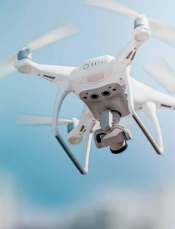
72
73 MOSFETs 4 Automotive MOSFETs...74 Automotive grade MOSFETs nomenclature N-channel 30V automotive power MOSFETs N-channel 40V automotive power MOSFETs N-channel 55V-60V automotive power MOSFETs N-channel 75V-80V automotive power MOSFETs N-channel 100V automotive power MOSFETs Small-signal automotive MOSFETs Low R DS(on) Small-signal automotive MOSFETs High R DS(on) Small-signal automotive MOSFETs Dual Power MOSFETs...86 N-channel 25V-30V MOSFETs N-channel 40V-60V MOSFETs N-channel 75V-200V MOSFETs P-channel MOSFETs Power MOSFETs nomenclature Small-signal MOSFETs...94 Small-signal MOSFETs in DFN1006 and DFN1006B packages Small-signal MOSFETs in DFN1010D-3 single and DFN1010B-3 dual packages Small-signal low-leakage MOSFETs Small-signal MOSFETs in DFN2020MD-6 single and DFN dual packages Small-signal MOSFETs in WLCSP4 and WLCSP6 packages Small-signal MOSFETs single (N-channel) Small-signal MOSFETs single (P-channel) Small-signal MOSFET Schottky combination Small-signal MOSFETs dual Small-signal MOSFETs complementary
74 Automotive MOSFETs Automotive grade MOSFETs nomenclature BUK 7 Y 3R0-40 H Segment 'BUK' for automotive grade Gate drive 7 = Standard level 6 = Intermediate level 9 = Logic level Package 6 = D2PAK 2 = DPAK E = I2PAK 5 = TO-220 M = LFPAK33 Y = LFPAK56 K = LFPAK56D J = LFPAK56E TrenchMOS technology A = Generation 2 B = Generation 3 C = Generation 4 E = Generation 6 H = Generation 9 Voltage rating BV DSS rating 3R0 = R DS(on) <3mΩ max at 25 o C N-channel 30V automotive power MOSFETs Package name V DS [max] (V) R DS(on) 10 V (mω) R DS(on) 5 V (mω) I D 25 C (A) R th(j-mb) [max] (K/W) BUK962R8-30B D 2 PAK (SOT404) BUK762R7-30B BUK763R4-30B BUK B BUK B BUK9Y07-30B BUK7Y07-30B LFPAK56; Power-SO8 (SOT669) BUK9Y11-30B BUK7Y10-30B BUK9Y22-30B BUK7Y20-30B BUK9K5R1-30E LFPAK56D (SOT1205) BUK9K5R6-30E BUK7K5R1-30E BUK7K5R6-30E BUK9M5R2-30E LFPAK33 (SOT1210) BUK9M6R6-30E BUK9M10-30E BUK9M17-30E Nexperia selection guide 2018
75 Automotive MOSFETs N-channel 40V automotive power MOSFETs Types in bold represent new products Package name V DS [max] (V) R DS(on) 10 V (mω) R DS(on) 5 V (mω) I D 25 C (A) R th(j-mb) [max] (K/W) BUK751R8-40E TO-220AB (SOT78) D 2 PAK (SOT404) DPAK (SOT428) I 2 PAK (SOT226) LFPAK56E (SOT1023) BUK752R3-40E BUK753R1-40E BUK758R3-40E BUK961R6-40E BUK761R6-40E BUK761R7-40E BUK762R0-40E BUK962R6-40E BUK762R6-40E BUK963R1-40E BUK762R9-40E BUK964R1-40E BUK764R0-40E BUK965R4-40E BUK765R3-40E BUK768R1-40E BUK B BUK B BUK7E1R8-40E BUK7E1R9-40E BUK7E2R3-40E BUK7E3R1-40E BUK7E8R3-40E BUK7J1R4-40H 40 1, ,38 BUK7Y1R7-40H 40 1, ,51 LFPAK56; Power-SO8 (SOT669) LFPAK56D (SOT1205) BUK7Y2R0-40H ,69 BUK7Y2R5-40H 40 2, ,79 BUK7Y3R0-40H ,87 BUK9Y3R0-40E BUK7Y3R5-40E BUK9Y3R5-40E BUK9Y4R4-40E BUK7Y4R4-40E BUK9Y7R6-40E BUK7Y7R6-40E BUK9Y12-40E BUK7Y12-40E BUK9Y21-40E BUK7Y21-40E BUK9Y29-40E BUK7Y29-40E BUK7K6R2-40E BUK9K6R2-40E BUK9K6R8-40E BUK7K6R8-40E BUK9K8R7-40E BUK7K8R7-40E BUK9K18-40E BUK7K18-40E BUK9K25-40E BUK7K25-40E MOSFETs 75
76 Automotive MOSFETs N-channel 40V automotive power MOSFETs Package name V DS [max] (V) R DS(on) 10 V (mω) R DS(on) 5 V (mω) I D 25 C (A) R th(j-mb) [max] (K/W) BUK7M6R3-40E BUK7M8R0-40E BUK7M10-40E BUK7M12-40E BUK7M21-40E LFPAK33 (SOT1210) BUK7M45-40E BUK9M14-40E BUK9M24-40E BUK9M52-40E BUK9M7R2-40E BUK9M9R1-40E BUK9M11-40E N-channel 55V-60V automotive power MOSFETs Package name V DS [max] (V) R DS(on) 10 V (mω) R DS(on) 5 V (mω) I D 25 C (A) R th(j-mb) [max] (K/W) TO-220AB (SOT78) BUK953R5-60E BUK954R8-60E BUK AL BUK A BUK A BUK A D2PAK (SOT404) BUK A BUK A BUK A BUK A BUK A BUK A BUK A BUK962R5-60E BUK762R4-60E BUK962R8-60E BUK762R6-60E BUK963R3-60E BUK763R1-60E BUK964R2-60E D 2 PAK (SOT404) BUK763R9-60E BUK964R8-60E BUK764R4-60E BUK966R5-60E BUK766R0-60E BUK969R0-60E BUK768R3-60E BUK E BUK E Nexperia selection guide 2018
77 Automotive MOSFETs N-channel 55V-60V automotive power MOSFETs Package name V DS [max] (V) R DS(on) 10 V (mω) R DS(on) 5 V (mω) I D 25 C (A) R th(j-mb) [max] (K/W) BUK B BUK B BUK B DPAK (SOT428) BUK A BUK A BUK A BUK A BUK A BUK A BUK A BUK A BUK A BUK A DPAK (SOT428) BUK A BUK A BUK A BUK A BUK A BUK A BUK A BUK7E2R6-60E I 2 PAK (SOT226) BUK7E3R5-60E BUK7E4R6-60E BUK7E13-60E BUK9Y4R8-60E MOSFETs LFPAK56; Power-SO8 (SOT669) BUK7Y4R8-60E BUK9Y6R0-60E BUK9Y7R2-60E BUK7Y6R0-60E BUK7Y7R2-60E BUK9Y8R7-60E BUK7Y8R7-60E BUK9Y15-60E BUK7Y15-60E BUK9Y25-60E BUK7Y25-60E BUK9Y43-60E BUK7Y43-60E BUK9Y59-60E BUK7Y59-60E
78 Automotive MOSFETs N-channel 55V-60V automotive power MOSFETs Package name V DS [max] (V) R DS(on) 10 V (mω) R DS(on) 5 V (mω) I D 25 C (A) R th(j-mb) [max] (K/W) BUK7K12-60E BUK7K13-60E BUK9K12-60E BUK9K13-60E LFPAK56D (SOT1205) BUK7K17-60E BUK9K17-60E BUK7K35-60E BUK9K35-60E BUK7K52-60E BUK9K52-60E BUK7M9R9-60E BUK9M12-60E BUK7M12-60E BUK9M15-60E BUK7M15-60E BUK9M19-60E LFPAK33 (SOT1210) BUK7M19-60E BUK9M24-60E BUK7M33-60E BUK9M42-60E BUK7M42-60E BUK9M53-60E BUK7M67-60E BUK9M85-60E BUK A/CU BUK A/CU SOT223 BUK A/CU BUK A/CU BUK A/CU Nexperia selection guide 2018
79 Automotive MOSFETs N-channel 75V-80V automotive power MOSFETs Package name V DS [max] (V) R DS(on) 10 V (mω) R DS(on) 5 V (mω) I D 25 C (A) R th(j-mb) [max] (K/W) TO-220AB (SOT78) BUK753R8-80E BUK B BUK B BUK A D 2 PAK (SOT404) BUK763R8-80E BUK964R2-80E BUK764R2-80E BUK964R7-80E BUK769R6-80E BUK E BUK B DPAK (SOT428) BUK B BUK A BUK A BUK7Y7R8-80E BUK9Y8R5-80E BUK7Y9R9-80E BUK9Y11-80E BUK9Y14-80E BUK7Y14-80E LFPAK56; Power-SO8 (SOT669) BUK9Y25-80E BUK7Y25-80E BUK9Y41-80E BUK7Y41-80E BUK9Y72-80E MOSFETs LFPAK56D (SOT1205) LFPAK33 (SOT1210 BUK7Y72-80E BUK9Y107-80E BUK7Y98-80E BUK7K15-80E BUK7K17-80E BUK7K23-80E BUK9K20-80E BUK9K22-80E BUK9K30-80E BUK7M17-80E BUK9M23-80E BUK7M22-80E BUK7M27-80E BUK9M28-80E BUK9M35-80E
80 Automotive MOSFETs N-channel 100V automotive power MOSFETs Package name V DS [max] (V) R DS(on) 10 V (mω) R DS(on) 5 V (mω) I D 25 C (A) R th(j-mb) [max] (K/W) TO-220AB (SOT78) BUK755R4-100E BUK765R0-100E BUK965R8-100E BUK768R1-100E BUK969R3-100E BUK E BUK E D2PAK (SOT404) BUK E BUK E BUK A BUK A BUK A BUK A BUK A BUK B BUK B DPAK (SOT428) BUK A BUK A BUK A BUK A I 2 PAK (SOT226) BUK7E5R2-100E BUK9Y12-100E BUK7Y12-100E BUK9Y15-100E BUK7Y15-100E BUK9Y19-100E BUK7Y19-100E BUK9Y22-100E LFPAK56; Power-SO8 (SOT669) BUK7Y22-100E BUK9Y38-100E BUK7Y38-100E BUK9Y65-100E BUK7Y65-100E BUK9Y E BUK7Y E BUK9Y E BUK7Y E Nexperia selection guide 2018
81 Automotive MOSFETs N-channel 100V automotive power MOSFETs Package name V DS [max] (V) R DS(on) 10 V (mω) R DS(on) 5 V (mω) I D 25 C (A) R th(j-mb) [max] (K/W) BUK7K29-100E BUK9K29-100E BUK7K32-100E BUK9K32-100E LFPAK56D (SOT1205) BUK7K45-100E BUK9K45-100E BUK7K89-100E BUK9K89-100E BUK7K E BUK9K E BUK9M34-100E LFPAK33 (SOT1210) BUK9M43-100E BUK9M E BUK9M E SOT223 BUK A/CU BUK A/CU P-channel 30V-60V automotive power MOSFETs Types in bold red are in development MOSFETs Package name V DS [max] (V) R DS(on) 10 V (mω) I D 25 C (A) R th(j-mb) [max] (K/W) BUK6Y12-30P BUK6Y20-30P LFPAK56 BUK6Y15-40P BUK6Y25-40P BUK6Y32-60P BUK6Y57-60P
82 Automotive MOSFETs Small-signal automotive MOSFETs Low R DS(on) Package Size (mm) P tot (mw) Polarity V DS (V) V GS (V) I D (A) V GS(th) V GS(th) ESD protection R DS(on) typ V GS = min (V) max (V) (kv) 10 V 4.5 V 2.5 V 1.8 V ,47 0,9 2, ,8 1 2, N-channel P-channel 82 Nexperia selection guide 2018
83 Automotive MOSFETs Types in bold represent new products SOT223 SOT457 (SC-74) SOT23 SOT323 (SC-70) DFN2020MD-6 (SOT1220) DFN2020D-6 (SOT1118D) DFN1010D-3 (SOT1215) 6.5 x 3.5 x x 1.5 x x 1.3 x x 1.25 x x 2.0 x x 2.0 x x 1.0 x PMV28UNEA PMF63UNEA PMV65UNEA PMPB10XNEA PMPB12UNEA PMV20XNEA PMPB20XNEA PMPB13XNEA PMPB29XNEA PMDPB56XNEA PMF250XNEA PMV25ENEA PMV50ENEA PMV100ENEA BUK9D23-40E PMV65ENEA PMV130ENEA BUK6D23-40E BUK7D25-40E PMPB55ENEA PMV55ENEA PMPB85ENEA PMV120ENEA PMV230ENEA PMV450ENEA BUK6D43-60E MOSFETs PMPB95ENEA PMPB215ENEA PMXB360ENEA PMT280ENEA PMV280ENEA PMT560ENEA PMPB15XPA PMV27UPEA PMN40UPEA NX2301P BSH205G2 PMPB20XPEA PMN27XPEA PMPB29XPEA PMV30XPEA PMPB43XPEA PMN42XPEA PMV48XPA PMV65XPEA PMN70XPEA PMV100XPEA PMPB27EPA PMV50EPEA PMPB50EPEA PMV250EPEA PMPB45EPA BUK6D43-40P PMT200EPEA 83
84 Automotive MOSFETs Small-signal automotive MOSFETs High R DS(on) Package Size (mm) P tot (mw) Polarity V DS (V) V GS (V) I D (A) V GS(th) V GS(th) ESD protection R DS(on) typ V GS = min (V) max (V) (kv) 10 V 4.5 V 2.5 V 1.8 V N yes P Small-signal automotive MOSFETs Dual Package Size (mm) P tot (mw) V Polarity V DS (V) V GS (V) I D (A) GS(th) V GS(th) ESD protection R DS(on) typ V GS = min (V) max (V) (kv) 10 V 4.5 V 2.5 V 1.8 V N P N P Nexperia selection guide 2018
85 Automotive MOSFETs SOT23 SOT363 (SC-88) SOT323 (SC-70) SOT666 DFN1006 (SOT883) 2.9 x 1.3 x x 1.25 x x 1.25 x x 1.2 x x 0.6 x NX3008NBK NX3008NBKS NX3008NBKW NX3008NBKV BSS138P BSS138PS BSS138PW BSS138BK BSS138BKS BSS138BKW 2N7002BK 2N7002BKS 2N7002BKW 2N7002BKM 2N7002CK BSS138AKA NX3008PBK NX3008PBKS NX3008PBKW NX3008PBKV BSS84AK BSS84AKS BSS84AKW BSS84AKV BSS84AKM SOT363 (SC-88) SOT666 DFN2020D-6 (SOT1118D) 2.0 x 1.25 x x 1.2 x x 2.0 x PMDT290UNE PMGD175XNEA PMDT670UPE PMDPB56XNEA MOSFETs PMGD290UCEA 85
86 Power MOSFETs N-channel 25V-30V MOSFETs Types in bold red are in development Package V DS [max] (V) R DS(on) V GS = 10 V (mω) R DS(on) V GS = 4.5 V or 5 V (mω) I D [max] (A) Q G(tot) [typ] (nc) PSMN1R1-30PL PSMN1R6-30PL PSMN1R8-30PL TO-220 (SOT78) PSMN2R0-30PL PSMN2R7-30PL PSMN3R4-30PL PSMN4R3-30PL PSMN017-30PL PSMN022-30PL PSMNR90-30BL PSMN1R5-30BLE PSMN1R8-30BL PSMN1R6-30BL D 2 PAK (SOT404) PSMN2R0-30BL PSMN2R7-30BL PSMN3R4-30BL PSMN3R4-30BLE PSMN4R3-30BL PSMN017-30BL PSMN022-30BL I 2 PAK (SOT226) PSMN1R1-30EL PSMN017-30EL PSMNR51-25YLH PSMNR60-25YLH PSMN0R7-25YLD PSMN0R9-25YLD PSMN1R0-25YLD PSMN1R1-25YLC PSMN1R2-25YLD LFPAK56 (Power-SO8) PSMN1R2-25YL PSMN1R2-25YLC PSMN1R5-25YL PSMN1R7-25YLD PSMN2R0-25YLD PSMN2R9-25YLC PSMN4R0-25YLC PSMN5R4-25YLD PSMN6R0-25YLD PSMN6R0-25YLB Nexperia selection guide 2018
87 Power MOSFETs N-channel 25V-30V MOSFETs Types in bold red are in development Package V DS [max] (V) R DS(on) V GS = 10 V (mω) R DS(on) V GS = 4.5 V or 5 V (mω) I D [max] (A) Q G(tot) [typ] (nc) PSMNR58-30YLH PSMNR70-30YLH PSMN0R9-30YLD PSMN1R0-30YLD PSMN1R0-30YLC PSMN1R2-30YLD PSMN1R2-30YLC PSMN1R3-30YL PSMN1R4-30YLD PSMN1R5-30YL PSMN1R5-30YLC PSMN1R7-30YL PSMN2R0-30YLD PSMN2R0-30YL PSMN2R0-30YLE PSMN2R2-30YLC PSMN2R4-30YLD PSMN2R5-30YL PSMN2R6-30YLC LFPAK56 (Power-SO8) PSMN3R0-30YL PSMN3R0-30YLD PSMN3R5-30YL PSMN4R0-30YL PSMN4R0-30YLD PSMN4R1-30YLC PSMN5R0-30YL PSMN6R0-30YL MOSFETs PSMN6R0-30YLD PSMN6R1-30YLD PSMN6R0-30YLB PSMN7R0-30YL PSMN7R0-30YLC PSMN7R5-30YLD PSMN9R1-30YL PSMN9R5-30YLC PSMN013-30YLC PSMN011-30YLC PSMN3R2-30YLC PSMN4R5-30YLC
88 Power MOSFETs N-channel 25V-30V MOSFETs Types in bold red are in development Package V DS [max] (V) R DS(on) V GS = 10 V (mω) R DS(on) V GS = 4.5 V or 5 V (mω) I D [max] (A) Q G(tot) [typ] (nc) PSMN2R0-25MLD PSMN2R8-25MLC PSMN3R5-25MLD PSMN3R9-25MLC PSMN5R3-25MLD PSMN6R1-25MLD PSMN9R0-25MLC PSMN1R6-30MLH LFPAK33 (SOT1210) PSMN2R4-30MLD PSMN3R0-30MLC PSMN4R2-30MLD PSMN4R4-30MLC PSMN6R4-30MLD PSMN6R5-30MLD PSMN7R0-30MLC PSMN7R5-30MLD PSMN9R8-30MLC PSMN013-30MLC PSMN020-30MLC N-channel 40V-60V MOSFETs Package V DS [max] (V) R DS(on) V GS = 10 V (mω) R DS(on) V GS = 4.5 V or 5 V (mω) I D [max] (A) Q G(tot) [typ] (nc) PSMN1R5-40PS PSMN1R9-40PL PSMN2R2-40PS PSMN2R1-40PL PSMN2R8-40PS PSMN4R5-40PS PSMN8R0-40PS PSMN2R0-60PSR TO-220 (SOT78) PSMN2R0-60PS PSMN2R5-60PL PSMN2R6-60PS PSMN3R0-60PS PSMN3R3-60PL PSMN4R2-60PL PSMN3R9-60PS PSMN4R6-60PS PSMN7R6-60PS PSMN015-60PS Nexperia selection guide 2018
89 Power MOSFETs N-channel 40V-60V MOSFETs Package V DS [max] (V) R DS(on) V GS = 10 V (mω) R DS(on) V GS = 4.5 V or 5 V (mω) I D [max] (A) Q G(tot) [typ] (nc) PSMN1R1-40BS PSMN2R2-40BS PSMN2R8-40BS PSMN4R5-40BS D 2 PAK (SOT404) PSMN8R0-40BS PSMN1R7-60BS PSMN3R0-60BS PSMN4R6-60BS PSMN7R6-60BS PSMN015-60BS I 2 PAK (SOT226) PSMN1R5-40ES PSMN2R0-60ES PSMN3R0-60ES PSMN1R0-40YLD PSMN1R4-40YLD PSMN1R8-40YLC PSMN2R6-40YS PSMN3R3-40YS PSMN4R0-40YS PSMN5R8-40YS PSMN8R3-40YS PSMN014-40YS LFPAK56 (Power-SO8) PSMN4R0-60YS PSMN4R1-60YL PSMN5R2-60YL PSMN5R5-60YS PSMN5R6-60YL MOSFETs LFPAK33 (SOT1210) PSMN7R0-60YS PSMN7R5-60YL PSMN8R5-60YS PSMN012-60YS PSMN013-60YL PSMN030-60YS PSMN017-60YS PSMN011-60ML PSMN011-60MS
90 Power MOSFETs N-channel 75V-200V MOSFETs Types in bold represent new products Package V DS [max] (V) R DS(on) V GS = 10 V (mω) R DS(on) V GS = 4.5 V or 5 V (mω) I D [max] (A) Q G(tot) [typ] (nc) PSMN3R3-80PS PSMN3R5-80PS PSMN4R4-80PS PSMN4R3-80PS PSMN5R0-80PS PSMN6R5-80PS PSMN8R7-80PS PSMN012-80PS PSMN017-80PS PSMN4R3-100PS PSMN4R8-100PSE PSMN5R0-100PS PSMN5R6-100PS PSMN7R0-100PS PSMN7R8-100PSE PSMN8R5-100PS PSMN8R5-100PSF TO-220 (SOT78) PSMN9R5-100PS PSMN PS PSMN PS PSMN PSF PSMN PS PSMN PS PSMN P PHP27NQ11T PHP23NQ11T PHP18NQ11T PSMN6R3-120PS PSMN7R8-120PS PSMN P PHP30NQ15T PHP28NQ15T PSMN P PHP33NQ20T PHP20NQ20T PHP9NQ20T PSMN2R8-80BS D 2 PAK (SOT404) PSMN3R3-80BS PSMN4R4-80BS PSMN5R0-80BS Nexperia selection guide 2018
91 Power MOSFETs N-channel 75V-200V MOSFETs Types in bold represent new products Package V DS [max] (V) R DS(on) V GS = 10 V (mω) R DS(on) V GS = 4.5 V or 5 V (mω) I D [max] (A) Q G(tot) [typ] (nc) PSMN6R5-80BS PSMN8R7-80BS PSMN012-80BS PSMN017-80BS PSMN050-80BS PSMN3R8-100BS PSMN4R8-100BSE PSMN5R6-100BS PSMN7R0-100BS D 2 PAK (SOT404) PSMN7R0-100BSF PSMN7R6-100BSE PSMN9R5-100BS PSMN BS PSMN BS PSMN BSF PSMN BS PSMN BS PHB45NQ15T PSMN B PHB33NQ20T PHB20NQ20T DPAK (SOT428) PSMN D PSMN D PHD9NQ20T PSMN3R3-80ES PSMN3R5-80ES PSMN4R3-80ES MOSFETs I 2 PAK (SOT226) PSMN4R3-100ES PSMN5R0-100ES PSMN7R0-100ES PSMN8R5-100ES PSMN8R5-100ESF PSMN ES PSMN ESF PSMN6R3-120ES PSMN7R8-120ES Types in bold red are in development 91
92 Power MOSFETs N-channel 75V-200V MOSFETs Types in bold represent new products Package V DS [max] (V) R DS(on) V GS = 10 V (mω) R DS(on) V GS = 4.5 V or 5 V (mω) I D [max] (A) Q G(tot) [typ] (nc) PSMN8R0-80YL PSMN8R2-80YS PSMN010-80YL PSMN011-80YS PSMN013-80YS PSMN014-80YL PSMN018-80YS PSMN025-80YL PSMN026-80YS PSMN041-80YL PSMN045-80YS PSMN5R6-100YSF PSMN6R9-100YSF LFPAK56 (Power-SO8) PSMN8R7-100YSF PSMN YL PSMN YS PSMN YSE PSMN YL PSMN YS PSMN YL PSMN YL PSMN YS PSMN YS PSMN YL PSMN YS PSMN YS PSMN Y PSMN Y LFPAK33 (SOT1210) SOT873 PSMN MSE PSMN MSE PML260SN PML340SN P-channel MOSFETs Package V DS [max] (V) R DS(on) V GS = 10 V (mω) I D [max] (A) Q G(tot) [typ] (nc) PSMP012-30YE PSMP020-30YE PSMP015-40YE LFPAK56 PSMP025-40YE PSMP032-60YE PSMP057-60YE Types in bold red are in development 92 Nexperia selection guide 2018
93 Power MOSFETs Power MOSFETs nomenclature PSM N 4R0-30 Y L D Segment Power silicon max Voltage rating BV DSS rating Channel N = N-channel P = P-channel X = Dual R DS(on) in mω 4R0 means 4mΩ max at 25 o C Package type B = D 2 PAK D = DPAK E = I 2 PAK K = S08 L = DFN56AD P = TO220 Y = LFPAK56 M = LFPAK33 Gate threshold voltage L = Logic level S = Standard level U = Ultra low gate X = Extremely low gate E = Enhanced logic Technology family, e.g. C = NextPower D = NextPowerS3 (Super-fast Switching with Soft Recovery) E = NextPower Live (optimized for hotswap applications) F = NextPower 80/100 V MOSFETs 93
94 Small-signal MOSFETs Small-signal MOSFETs in DFN1006 and DFN1006B packages Package DFN (SOT883) DFN1006B-3 (SOT883B) Size (mm) 1.0 x 0.6 x x 0.6 x 0.37 Ptot (mw) Polarity V DS (V) V GS (V) I D (A) V GS(th) min (V) V GS(th) max (V) t on typ (ns) t off typ (ns) Q G typ (nc) ESD protection (kv) R DS(on) typ V GS = 10 V 4.5 V 2.5 V 1.8 V 1.5 V 1.2 V PMZ130UNE PMZB150UNE PMZ290UNE2 PMZB290UNE2 N-channel PMZ600UNE PMZB600UNE PMZ200UNE PMZB200UNE PMZ390UNE PMZB390UNE PMZ550UNE PMZB550UNE N700BKM 2N7002BKMB NX7002BKM NX7002BKMB P-channel PMZ350UPE PMZB350UPE PMZ950UPE PMZB950UPE PMZ320UPE PMZB320UPE PMZ1200UPE PMZB1200UPE BSS84AKM BSS84AKMB 94 Nexperia selection guide 2018
95 Small-signal MOSFETs Small-signal MOSFETs in DFN1010D-3 single and DFN1010B-3 dual packages Package DFN1010D-3 (SOT1215) DFN1010B-6 (SOT1216) Size (mm) 1.1 x 1.0 x x 1.0 x 0.37 P tot (mw) Configuration Polarity V DS (V) V GS (V) I D (A) V GS(th) min (V) V GS(th) max (V) t on typ (ns) t off typ (ns) Q G typ (nc) ESD protection (kv) R DS(on) typ V GS = 10 V 4.5 V 2.5 V 1.8 V 1.5 V 1.2 V Single Dual Complementary P-channel N-channel N-ch P-ch PMXB40UNE PMXB43UNE PMXB56EN PMXB65ENE PMXB360ENEA PMXB65UPE PMXB75UPE PMXB350UPE PMXB120EPE PMDXB600UNE PMDXB550UNE NX7002BKXB PMDXB950UPE PMDXB1200UPE N PMCXB900UE P N PMCXB1000UE P Small-signal low-leakage MOSFETs Package DFN (SOT883) DFN1006B-3 (SOT883B) DFN1010B-6 (SOT1216) MOSFETs Size (mm) 1.0 x 0.6 x x 0.6 x x 1.0 x 0.37 Ptot (mw) Config. Polarity V DS (V) V GS (V) I D (A) V GS(th) min (V) V GS(th) max (V) I DSS max (na) I GSS max (na) ESD Protection (kv) R DS(on) typ V GS = 4.5 V 2.5 V 1.8 V 1.5 V 1.2 V N PMZ600UNEL PMZB600UNEL Single P PMZ950UPEL PMZB950UPEL N PMDXB600UNEL Dual P PMDXB950UPEL N Compl. PMCXB900UEL P
96 Small-signal MOSFETs Small-signal MOSFETs in DFN2020MD-6 single and DFN dual packages DFN2020MD-6 (SOT1220) DFN (SOT1118) Package Size (mm) 2.0 x 2.0 x x 2.0 x 0.65 P tot (mw) Configuration Polarity V DS (V) V GS (V) I D (A) V GS(th) min (V) V GS(th) max (V) t on typ (ns) t off typ (ns) Q G typ (nc) ESD protection (kv) R DS(on) typ V GS = 10 V 4.5 V 2.5 V 1.8 V PMPB12UNE PMPB10XNE PMPB20XNEA PMPB15XN PMPB23XNE PMPB13XNE N-channel PMPB29XNE PMPB33XN PMPB11EN PMPB20EN Single PMPB55ENEA PMPB85ENEA PMPB95ENEA PMPB215ENEA PMPB15XP PMPB19XP PMPB20XPE P-channel PMPB29XPE PMPB33XP PMPB43XPE PMPB47XP PMPB27EP PMPB48EP PMDPB30XN N-ch PMDPB56XNEA PMDPB95XNE2 Dual PMDPB58UPE PMDPB85UPE P-channel PMDPB55XP PMDPB70XPE PMDPB80XP PMDPB70XP MOSFET- Schottky P-channel PMFPB8032XP Pre-biased NPN P PMC85XP Complementary N P PMCPB5530X 96 Nexperia selection guide 2018
97 Small-signal MOSFETs Small-signal MOSFETs in WLCSP4 and WLCSP6 packages Types in bold represent new products WLCSP4 WLCSP6 Package Size (mm) 0.78 x 0.78 x x 0.98 x 0.35 P tot (mw) Configuration Polarity V DS (V) V GS (V) I D (A) V GS(th) min (V) V GS(th) max (V) t on typ (ns) t off typ (ns) Q G typ (nc) ESD protection (kv) R DS(on) typ V GS = 4.5 V 2.5 V 1.8 V 1.5 V N PMCM4401VNE PMCM4401UNE PMCM4401VPE P PMCM4401UPE PMCM4402UPE N P PMCM6501VNE PMCM6501UNE PMCM6501VPE PMCM6501UPE Common drain N PMCM6501CUNE MOSFETs 97
98 Small-signal MOSFETs Small-signal MOSFETs single (N-channel) Package Size (mm) P tot (mw) V DS (V) V GS (V) I D (A) V GS(th) min (V) V GS(th) max (V) t on typ (ns) t off typ (ns) Q G typ (nc) ESD protection (kv) R DS(on) typ V GS = 10 V 4.5 V 2.5 V 1.8 V yes yes Nexperia selection guide 2018
99 Small-signal MOSFETs Types in bold represent new products SOT223 SOT457 (SC-74) SOT23 SOT323 (SC-70) DFN1006 (SOT883) DFN1006B (SOT883B) 6.5 x 3.5 x x 1.5 x x 1.3 x x 1.25 x x 0.6 x x 0.6 x PMV28UNEA PMF63UNE PMV65UNE PMZ130UNE PMZB150UNE PMZ290UNE2 PMZ600UNE PMZB290UNE2 PMZB600UNE PMV20XNEA PMV16XN PMN16XNE PMV30UN2 PMN30UNE PMZ200UNE PMZ390UNE PMZ550UNE PMZB200UNE PMZB390UNE PMZB550UNE NX3008NBK NX3008NBKW PMV20XNE PMN30UN PMV40UN2 PMV20EN PMV25ENEA PMF250XNE MOSFETs PMV50ENEA PMV37EN2 PMN40ENE PMV42ENE PMV45EN2 PMV90ENE NX3020NAK NX3020NAKW PMV65ENEA PMV130ENEA BSH111BK PMV55ENEA PMV120ENEA PMV230ENEA PMV450ENEA NX138AK NX138BK NX138AKW NX138BKW BSN20BK NX7002AK NX7002AKW NX7002BK NX7002BKW NX7002BKM NX7002BKMB PMT280ENEA PMV280ENEA PMT560ENEA 99
100 Small-signal MOSFETs Small-signal MOSFETs single (P-channel) Package Size (mm) P tot (mw) V DS (V) V GS (V) I D (A) V GS(th) min (V) V GS(th) max (V) t on typ (ns) t off typ (ns) Q G typ (nc) ESD protection (kv) R DS(on) typ V GS = 10 V 4.5 V 2.5 V 1.8 V / Small-signal MOSFET Schottky combination Package DFN (SOT1118) Size (mm) 2.0 x 2.0 x 0.65 P tot (mw) 1250 Configuration V DS (V) V GS (V) I D (A) V GS(th) min (V) V GS(th) max (V) t on typ (ns) t off typ (ns) Q G typ (nc) I F (A) V R (V) V F typ. (mv) R DS(on) typ V GS = 4.5 V 2.5 V 1.8 V Single + schottky PMFPB8040XP 100 Nexperia selection guide 2018
101 Small-signal MOSFETs Types in bold represent new products SOT223 SOT457 (SC-74) SOT23 SOT363 (SC-88) SOT323 (SC-70) DFN (SOT883) DFN1006B-3 (SOT883B) 6.5 x 3.5 x x 1.5 x x 1.3 x x 1.25 x x 1.25 x x 0.6 x x 0.6 x PMV27UPE PMV33UPE PMV32UP PMV50UPE NX2301P PMV160UP BSH205G2 PMN30XP PMV30XPEA PMZ350UPE PMZ950UPE PMZB350UPE PMZB950UPE PMT200EPEA PMN48XP PMV48XP PMV50XP PMN52XP PMV65XP PMV65XPE PMN70XPE PMN70XP PMV75UP PMG85XP PMV100XPEA PMF170XP PMZ320UPE PMZB320UPE PMZ1200UPE PMZB1200UPE NX3008PBK NX3008PBKW PMV35EPE PMN70EPE PMV250EPEA BSS84AK BSS84AKW BSS84AKM BSS84AKMB MOSFETs 101
102 Small-signal MOSFETs Small-signal MOSFETs dual Package Size (mm) P tot (mw) Polarity V DS (V) V GS (V) I D (A) V GS(th) min (V) V GS(th) max (V) t on typ (ns) t off typ (ns) Q G typ (nc) ESD protection (kv) N-channel P-channel yes yes yes Small-signal MOSFETs complementary Package Type Polarity SOT666 (1.6 x 1.2 x 0.55) NX1029X NX3008CBKV PMDT290UCE V DS (V) V GS (V) I D (A) V GSth min (V) V GSth max (V) N P N P N P SOT363 (SC-88) (2.0 x 1.25 x 0.95) DFN1010B-6 (1.1 x 1.0 x 0.37) DFN (2.0 x 2.0 x 0.65) NX3008CBKS PMCXB900UE PMCXB1000UE PMCPB5530X N P N P N P N P Nexperia selection guide 2018
103 Small-signal MOSFETs SOT363 (SC-88) SOT666 DFN (SOT1118) DFN1010B-6 (SOT1216) 2.0 x 1.25 x x 1.2 x x 2.0 x x 1.0 x R DS(on) typ V GS = 10 V 4.5 V 2.5 V 1.8 V PMDT290UNE PMDXB600UNE PMDPB30XN PMDXB550UNE NX3008NBKS NX3008NBKV PMDPB56XNEA PMDPB95XNE PMGD175XNE NX3020NAKS NX3020NAKV NX138AKS NX138BKS NX7002AKS NX7002BKS NX7002BKXB PMDT670UPE PMDPB58UPE PMDXB950UPE PMDPB85UPE PMDPB55XP PMDPB70XPE PMDPB80XP PMDXB1200UPE NX3008PBKS NX3008PBKV PMDPB70XP BSS84AKS BSS84AKV MOSFETs t on typ (ns) t off typ (ns) Q G typ ESD R DS(on) typ V GS = (nc) protection (kv) 10 V 4.5 V 2.5 V 1.8 V 1.5 V 1.2 V

104
105 Logic 5 Automotive logic Buffers, Drivers, Transceivers Buffers/Inverters/Drivers Transceivers Schmitt-triggers Counters/Frequency dividers Flip-flops, Latches, Registers FIFO registers Flip-flops Latches/Registered drivers Gates AND Gates Combination Gates Configurable Gates EXCLUSIVE-NOR Gates EXCLUSIVE-OR Gates NAND Gates NOR Gates OR Gates Logic voltage translators Level shifters/translators Specialty logic Digital comparators Multivibrators Parity generators-checkers Phase-locked loops Printer interfaces Switches, Multiplexers, Demultiplexers Bus Switches Decoders/Demultiplexers Digital Multiplexers Analog Switches Nomenclatures...161
106 Automotive logic Q100 Standard logic functions and packages Analog switches Features Package (suffix) Description Configuration V CC (V) R ON (W) R ON (FLAT) (W) T amb ( C) SOT108-1 (D) SOT402-1 (PW) SOT762-1 (BQ) SOT109-1 (D) SOT403-1 (PW) SOT763-1 (BQ) SOT137-1 (D) SOT355-1 (PW) SOT815-1 (BQ) 74HC4051-Q100 Single-pole, octal-throw analog switch SP8T-Z ~125 74HCT4051-Q100 Single-pole, octal-throw analog switch; TTL-enabled SP8T-Z ~125 74HC4052-Q100 Dual single-pole, quad-throw analog switch SP4T-Z ~125 74HCT4052-Q100 Dual single-pole, quad-throw analog switch; TTL-enabled SP4T-Z ~125 74HC4053-Q100 Triple single-pole, double-throw analog switch SP8T-Z ~125 74HCT4053-Q100 Triple single-pole, double-throw analog switch; TTL-enabled SP8T-Z ~125 74HC4066-Q100 Quad single-pole, single-throw analog switch SPST-NO ~125 74HCT4066-Q100 Quad single-pole, single-throw analog switch; TTL-enabled SPST-NO ~125 74HC4067-Q100 Single-pole, 16-throw analog switch SP16T-Z ~125 74HCT4067-Q100 Single-pole, 16-throw analog switch; TTL-enabled SP16T-Z ~125 74HC4851-Q100 Single-pole, octal-throw analog switch SP8T-Z ~125 74HCT4851-Q100 Single-pole, octal-throw analog switch; TTL-enabled SP8T-Z ~125 74HC4852-Q100 Dual single-pole, quad-throw analog switch SP4T-Z ~125 74HCT4852-Q100 Dual single-pole, quad-throw analog switch; TTL-enabled SP4T-Z ~125 74LV4052-Q100 Dual single-pole, quad-throw analog switch SP4T-Z ~125 74LV4053-Q100 Triple single-pole, double-throw analog switch SPDT-Z ~125 74LVC4066-Q100 Quad single-pole, single-throw analog switch SPST-NO ~125 HEF4051B-Q100 Single-pole, octal-throw analog switch SP8T-Z ~85 HEF4052B-Q100 Dual single-pole, quad-throw analog switch SP4T-Z ~85 HEF4053B-Q100 Triple single-pole, double-throw analog switch SPDT-Z ~85 HEF4066B-Q100 Quad single-pole, single-throw analog switch SPST-NO ~85 HEF4067B-Q100 Single-pole, 16-throw analog switch SP16T-Z ~ Nexperia selection guide 2018
107 Automotive logic Buffers/Inverters Features Package (suffix) Description V CC (V) I O (ma) t pd (ns) T amb ( C) SOT108-1 (D) SOT402-1 (PW) SOT762-1 (BQ) SOT109-1 (D) SOT403-1 (PW) SOT163-1 (D) SOT360-1 (PW) SOT764-1 (BQ) SOT362-1 (DGG) 74AHC04-Q100 Hex inverter ± ~125 74AHCT04-Q100 Hex inverter; TTL-enabled ± ~125 74AHC125-Q100 Quad buffer/line driver (3-state) ± ~125 74AHCT125-Q100 Quad buffer/line driver; TTL-enabled (3-state) ± ~125 74AHC126-Q100 Quad buffer/line driver (3-state) ± ~125 74AHCT126-Q100 Quad buffer/line driver; TTL-enabled (3-state) ± ~125 74AHC240-Q100 Octal inverter/line driver (3-state) ± ~125 74AHCT240-Q100 Octal inverter/line driver; TTL-enabled (3-state) ± ~125 74AHC244-Q100 Octal buffer/line driver (3-state) ± ~125 74AHCT244-Q100 Octal buffer/line driver; TTL-enabled (3-state) ± ~125 74AHC541-Q100 Octal buffer/line driver (3-state) ± ~125 74AHCT541-Q100 Octal buffer/line driver; TTL-enabled (3-state) ± ~125 74AHCU04-Q100 Hex inverter; unbuffered ± ~125 74ALVC125-Q100 Quad buffer/line driver (3-state) ± ~85 74ALVC541-Q100 Octal buffer/line driver (3-state) ± ~85 74HC05-Q100 Hex inverter; open-drain ~125 74HC04-Q100 Hex inverter ± ~125 74HCT04-Q100 Hex inverter; TTL-enabled ± ~125 74HC125-Q100 Quad buffer/line driver (3-state) ± ~125 74HCT125-Q100 Quad buffer/line driver; TTL-enabled (3-state) ± ~125 74HC126-Q100 Quad buffer/line driver (3-state) ± ~125 74HCT126-Q100 Quad buffer/line driver; TTL-enabled (3-state) ± ~125 74HC240-Q100 Octal inverter/line driver (3-state) ± ~125 74HCT240-Q100 Octal inverter/line driver; TTL-enabled (3-state) ± ~125 74HC244-Q100 Octal buffer/line driver (3-state) ± ~125 74HCT244-Q100 Octal buffer/line driver; TTL-enabled (3-state) ± ~125 74HC365-Q100 Hex buffer/line driver (3-state) ± ~125 Logic 74HCT365-Q100 Hex buffer/line driver; TTL-enabled (3-state) ± ~125 74HC366-Q100 Hex inverter/line driver (3-state) ± ~125 74HCT366-Q100 Hex inverter/line driver; TTL-enabled (3-state) ± ~125 74HC540-Q100 Octal inverter/line driver (3-state) ± ~125 74HCT540-Q100 Octal inverter/line driver; TTL-enabled (3-state) ± ~125 74HC541-Q100 Octal buffer/line driver (3-state) ± ~
108 Automotive logic Buffers/Inverters Features Package (suffix) Description V CC (V) I O (ma) t pd (ns) T amb ( C) SOT108-1 (D) SOT402-1 (PW) SOT762-1 (BQ) SOT109-1 (D) SOT403-1 (PW) SOT163-1 (D) SOT360-1 (PW) SOT764-1 (BQ) SOT362-1 (DGG) 74HCT541-Q100 Octal buffer/line driver; TTL-enabled (3-state) ± ~125 74HCU04-Q100 Hex inverter; unbuffered ± ~125 74LV244-Q100 Octal buffer/line driver (3-state) ± ~125 74LVC04A-Q100 Hex inverter ± ~125 74LVC06A-Q100 Hex inverter; open-drain ~125 74LVC07A-Q100 Hex buffer; open-drain ~125 74LVC125A-Q100 Quad buffer/line driver (3-state) ± ~125 74LVC126A-Q100 Quad buffer/line driver (3-state) ± ~125 74LVC541A-Q100 Octal buffer/line driver (3-state) ± ~125 74LVC16240A-Q bit inverter/line driver (3-state) ± ~125 74LVC244A-Q100 Octal buffer/line driver (3-state) ± ~125 74LVCH244A-Q100 Octal buffer/line driver with bus hold (3-state) ± ~125 74LVC16244A-Q bit buffer/line driver (3-state) ± ~125 74LVCH16244A-Q bit buffer/line driver with bus hold (3-state) ± ~125 74LVCU04A-Q100 Hex inverter; unbuffered ± ~125 74LVT04-Q100 Hex inverter / ~85 74LVT244A-Q100 Octal buffer/line driver with bus hold (3-state) / ~85 74LVTH244A-Q100 Octal buffer/line driver with bus hold (3-state) / ~85 74VHC126-Q100 Quad buffer/line driver (3-state) ± ~125 74VHCT126-Q100 Quad buffer/line driver; TTL-enabled (3-state) ± ~125 74VHC541-Q100 Octal buffer/line driver (3-state) ± ~125 74VHCT541-Q100 Octal buffer/line driver; TTL-enabled (3-state) ± ~125 HEF4049B-Q100 Hex inverter/line driver / ~85 HEF4050B-Q100 Hex buffer/line driver / ~85 HEF4069UB-Q100 Hex inverter; unbuffered ± ~ Nexperia selection guide 2018
109 Automotive logic Counters/Frequency dividers Types in bold represent new products Features Package (suffix) Description V CC (V) I O (ma) Logic t pd (ns) T amb ( C) SOT108-1 (D) SOT402-1 (PW) SOT762-1 (BQ) SOT109-1 (D) SOT403-1 (PW) SOT763-1 (BQ) 74HC161-Q100 Presettable synchronous 4-bit binary counter; asynchronous reset ± ~125 74HC163-Q100 Presettable synchronous 4-bit binary counter; synchronous reset ± ~125 74HCT163-Q100 Presettable synchronous 4-bit binary counter; synchronous reset; TTL-enabled ± ~125 74HC193-Q100 Presettable synchronous 4-bit binary up/down counter ± ~125 74HCT193-Q100 Presettable synchronous 4-bit binary up/down counter; TTL-enabled ± ~125 74HC393-Q100 Dual 4-bit binary ripple counter ± ~125 74HCT393-Q100 Dual 4-bit binary ripple counter; TTL-enabled ± ~125 74HC4017-Q100 Johnson decade counter with 10 decoded outputs ± ~125 74HCT4017-Q100 Johnson decade counter with 10 decoded outputs; TTL-enabled ± ~125 74HC4020-Q stage binary ripple counter ± ~125 74HCT4020-Q stage binary ripple counter; TTL-enabled ± ~125 74HC4024-Q100 7-stage binary ripple counter ± ~125 74HC4040-Q stage binary ripple counter ± ~125 74HCT4040-Q stage binary ripple counter; TTL-enabled ± ~125 74HC4060-Q stage binary ripple counter with oscillator ± ~125 74HCT4060-Q stage binary ripple counter with oscillator; TTL-enabled ± ~125 74HC4520-Q100 Dual 4-bit synchronous binary counter ± ~125 74HCT4520-Q100 Dual 4-bit synchronous binary counter; TTL-enabled ± ~125 74LV393-Q100 Dual 4-bit binary ripple counter ± ~125 HEF4017B-Q100 5-stage Johnson decade counter ± ~85 HEF4020B-Q stage binary ripple counter ± ~85 HEF4040B-Q stage binary ripple counter ± ~85 HEF4060B-Q stage binary ripple counter with oscillator ± ~85 HEF4541B-Q100 Programmable timer / ~85 HEF4520B-Q100 Dual 4-bit synchronous binary counter ± ~85 109
110 Automotive logic Bus switches Types in bold represent new products Features Package (suffix) Description V CC (V) V PASS (V) R ON (W) T amb ( C) SOT402-1 (PW) SOT762-1 (BQ) SOT109-1 (D) SOT403-1 (PW) SOT763-1 (BQ) SOT163-1 (D) SOT360-1 (PW) SOT764-1 (BQ) 74CBTLV3125-Q100 Quad bus switch ~125 74CBTLV3126-Q100 Quad bus switch ~125 74CBTLV3253-Q100 Dual 4:1 mux/demux ~125 74CBTLV3257-Q100 Quad 2:1 mux/demux ~125 74CBTLV3245-Q100 Octal bus switch ~125 74CBTLVD3245-Q100 Octal bus switch level translator ~125 CBT3245A-Q100 Octal bus switch ~85 Digital decoders/demultiplexers Features Package (suffix) Description V CC (V) I O (ma) t pd (ns) T amb ( C) SOT109-1 (D) SOT403-1 (PW) SOT763-1 (BQ) 74AHC138-Q100 3-to-8 line decoder/demultiplexer; inverting ± ~125 74AHCT138-Q100 3-to-8 line decoder/demultiplexer; inverting; TTL-enabled ± ~125 74AHC139-Q100 Dual 2-to-4 line decoder/demultiplexer ± ~125 74AHCT139-Q100 Dual 2-to-4 line decoder/demultiplexer; TTL-enabled ± ~125 74HC237-Q100 3-to-8 decoder/demultiplexer with address latches ± ~125 74HC138-Q100 3-to-8 line decoder/demultiplexer; inverting ± ~125 74HCT138-Q100 3-to-8 line decoder/demultiplexer; inverting; TTL-enabled ± ~125 74HC139-Q100 Dual 2-to-4 line decoder/demultiplexer ± ~125 74HCT139-Q100 Dual 2-to-4 line decoder/demultiplexer; TTL-enabled ± ~125 74HC238-Q100 3-to-8 decoder/demultiplexer ± ~125 74HCT238-Q100 3-to-8 decoder/demultiplexer; TTL-enabled ± ~125 74LVC138A-Q100 3-to-8 line decoder/demultiplexer; inverting ± ~125 HEF4555B-Q100 Dual 1-to-4 line decoder/demultiplexer ± ~ Nexperia selection guide 2018
111 Automotive logic Digital multiplexers Features Package (suffix) Description V CC (V) I O (ma) t pd (ns) T amb ( C) SOT109-1 (D) SOT403-1 (PW) SOT763-1 (BQ) 74AHC157-Q100 Quad 2-input multiplexer ± ~125 74AHCT157-Q100 Quad 2-input multiplexer; TTL-enabled ± ~125 74AHC257-Q100 Quad 2-input multiplexer (3-State) ± ~125 74AHCT257-Q100 Quad 2-input multiplexer; TTL-enabled (3-State) ± ~125 74HC151-Q100 8-input multiplexer ± ~125 74HCT151-Q100 8-input multiplexer; TTL-enabled ± ~125 74HC153-Q100 Dual 4-input multiplexer ± ~125 74HCT153-Q100 Dual 4-input multiplexer; TTL-enabled ± ~125 74HC157-Q100 Quad 2-input multiplexer ± ~125 74HCT157-Q100 Quad 2-input multiplexer; TTL-enabled ± ~125 74HC251-Q100 8-input multiplexer (3-State) ± ~125 74HCT251-Q100 8-input multiplexer; TTL-enabled (3-State) ± ~125 74HC253-Q100 Dual 4-input multiplexer (3-State) ± ~125 74HCT253-Q100 Dual 4-input multiplexer; TTL-enabled (3-State) ± ~125 74HC257-Q100 Quad 2-input multiplexer (3-State) ± ~125 74HCT257-Q100 Quad 2-input multiplexer; TTL-enabled (3-State) ± ~125 74LVC157A-Q100 Quad 2-input multiplexer ± ~125 Flip-flops Features Package (suffix) Description V CC (V) I O (ma) t pd (ns) T amb ( C) SOT108-1 (D) SOT402-1 (PW) SOT762-1 (BQ) SOT109-1 (D) SOT403-1 (PW) SOT163-1 (D) SOT360-1 (PW) SOT764-1 (BQ) SOT815-1 (BQ) SOT362-1 (DGG) 74AHC74-Q100 74AHCT74-Q100 74AHC273-Q100 74AHCT273-Q100 74AHC374-Q100 74AHCT374-Q100 74AHC377-Q100 74AHCT377-Q100 74AVC16374-Q100 Dual D-type flip-flop with set and reset; positive-edge trigger Dual D-type flip-flop with set and reset; positive-edge trigger; TTL-enabled Octal D-type flip-flop with reset; positive-edge trigger Octal D-type flip-flop with reset; positive-edge trigger; TTL-enabled Octal D-type flip-flop; positive-edge trigger Octal D-type flip-flop; positive-edge trigger (3-state); TTL-enabled (3-state) Octal D-type flip-flop with data enable; positive-edge trigger Octal D-type flip-flop with data enable; positive-edge trigger; TTL-enabled 16-bit D-type flip-flop; positive-edge trigger (3-state) ± ~ ± ~ ± ~ ± ~ ± ~ ± ~ ± ~ ± ~ ± ~85 Logic 111
112 Automotive logic Flip-flops Features Package (suffix) Description V CC (V) I O (ma) t pd (ns) T amb ( C) SOT108-1 (D) SOT402-1 (PW) SOT762-1 (BQ) SOT109-1 (D) SOT403-1 (PW) SOT163-1 (D) SOT360-1 (PW) SOT764-1 (BQ) SOT815-1 (BQ) SOT362-1 (DGG) 74HC74-Q100 Dual D-type flip-flop with set and reset; positive-edge trigger ± ~125 74HCT74-Q100 Dual D-type flip-flop with set and reset; positive-edge trigger; TTL-enabled ± ~125 74HC107-Q100 Dual J-K flip-flop with reset; negative-edge trigger ± ~125 74HCT107-Q100 Dual J-K flip-flop with reset; negative-edge trigger; TTL-enabled ± ~125 74HC109-Q100 Dual J-K flip-flop with set and reset; positive-edge trigger ± ~125 74HCT109-Q100 Dual J-K flip-flop with set and reset; positive-edge trigger; TTL-enabled ± ~125 74HC174-Q100 Hex D-type flip-flop with reset; positive-edge trigger ± ~125 74HCT174-Q100 Hex D-type flip-flop with reset; positive-edge trigger; TTL-enabled ± ~125 74HC175-Q100 Quad D-type flip-flop with reset; positive-edge trigger ± ~125 74HCT175-Q100 Quad D-type flip-flop with reset; positive-edge trigger; TTL-enabled ± ~125 74HC273-Q100 Octal D-type flip-flop with reset; positive-edge trigger ± ~125 74HCT273-Q100 Octal D-type flip-flop with reset; positive-edge trigger; TTL-enabled ± ~125 74HC377-Q100 Octal D-type flip-flop with data enable; positive-edge trigger ± ~125 74HCT377-Q100 Octal D-type flip-flop with data enable; positive-edge trigger; TTL-enabled ± ~125 74HC574-Q100 Octal D-type flip-flop; positive-edge trigger (3-state) ± ~125 74HCT574-Q100 Octal D-type flip-flop; positive-edge trigger; TTL-enabled (3-state) ± ~125 74LV74-Q100 Dual D-type flip-flop with set and reset; positive-edge trigger ± ~125 74LVC74A-Q100 Dual D-type flip-flop with set and reset; positive-edge trigger ± ~125 74LVC273-Q100 Octal D-type flip-flop with reset; positive-edge trigger ± ~125 74LVC374A-Q100 Octal D-type flip-flop; positive-edge trigger (3-state) ± ~ Nexperia selection guide 2018
113 Automotive logic Flip-flops Features Package (suffix) Description V CC (V) I O (ma) t pd (ns) T amb ( C) SOT108-1 (D) SOT402-1 (PW) SOT762-1 (BQ) SOT109-1 (D) SOT403-1 (PW) SOT163-1 (D) SOT360-1 (PW) SOT764-1 (BQ) SOT815-1 (BQ) SOT362-1 (DGG) 74LVC573A-Q100 Octal D-type transparent latch (3-state) ± ~125 74LVC823A-Q100 9-bit D-type flip-flop; positive-edge trigger (3-state) ± ~125 74LVC16374A-Q bit D-type flip-flop; positive-edge trigger (3-state) ± ~125 74LVCH16374A-Q bit D-type flip-flop with bus hold; positive-edge trigger (3-state) ± ~125 HEF4013B-Q100 Dual D-type flip-flop with set and reset; positive-edge trigger ± ~85 HEF4027B-Q100 Dual J-K flip-flop ± ~85 Gates Features Package (suffix) Description V CC (V) I O (ma) t pd (ns) T amb ( C) SOT108-1 (D) SOT402-1 (PW) SOT762-1 (BQ) 74AHC00-Q100 Quad 2-input NAND gate ± ~125 74AHCT00-Q100 Quad 2-input NAND gate; TTL-enabled ± ~125 74AHC02-Q100 Quad 2-input NOR gate ± ~125 74AHCT02-Q100 Quad 2-input NOR gate; TTL-enabled ± ~125 74AHC08-Q100 Quad 2-input AND gate ± ~125 74AHCT08-Q100 Quad 2-input AND gate; TTL-enabled ± ~125 74AHC30-Q100 8-input NAND gate ± ~125 Logic 74AHCT30-Q100 8-input NAND gate; TTL-enabled ± ~125 74AHC32-Q100 Quad 2-input OR gate ± ~125 74AHCT32-Q100 Quad 2-input OR gate; TTL-enabled ± ~125 74AHC86-Q100 Quad 2-input EXCLUSIVE-OR gate ± ~125 74AHCT86-Q100 Quad 2-input EXCLUSIVE-OR gate; TTL-enabled ± ~125 74ALVC00-Q100 Quad 2-input NAND gate ± ~85 113
114 Automotive logic Gates Features Package (suffix) Description V CC (V) I O (ma) t pd (ns) T amb ( C) SOT108-1 (D) SOT402-1 (PW) SOT762-1 (BQ) 74ALVC32-Q100 Quad 2-input OR gate ± ~125 74HC00-Q100 Quad 2-input NAND gate ± ~125 74HCT00-Q100 Quad 2-input NAND gate; TTL-enabled ± ~125 74HC02-Q100 Quad 2-input NOR gate ± ~125 74HCT02-Q100 Quad 2-input NOR gate; TTL-enabled ± ~125 74HC03-Q100 Quad 2-input NAND gate; open-drain ~125 74HCT03-Q100 Quad 2-input NAND gate; open-drain; TTL-enabled ± ~125 74HC08-Q100 Quad 2-input AND gate ± ~125 74HCT08-Q100 Quad 2-input AND gate; TTL-enabled ± ~125 74HC10-Q100 Triple 3-input NAND gate ± ~125 74HCT10-Q100 Triple 3-input NAND gate; TTL-enabled ± ~125 74HC11-Q100 Triple 3-input AND gate ± ~125 74HCT11-Q100 Triple 3-input AND gate; TTL-enabled ± ~125 74HC20-Q100 Dual 4-input NAND gate ± ~125 74HCT20-Q100 Dual 4-input NAND gate; TTL-enabled ± ~125 74HC27-Q100 Triple 3-input NOR gate ± ~125 74HCT27-Q100 Triple 3-input NOR gate; TTL-enabled ± ~125 74HC30-Q100 8-input NAND gate ± ~125 74HCT30-Q100 8-input NAND gate; TTL-enabled ± ~125 74HC32-Q100 Quad 2-input OR gate ± ~125 74HCT32-Q100 Quad 2-input OR gate; TTL-enabled ± ~125 74HC86-Q100 Quad 2-input EXCLUSIVE-OR gate ± ~125 74HCT86-Q100 Quad 2-input EXCLUSIVE-OR gate; TTL-enabled ± ~125 74HC4002-Q100 Dual 4-input NOR gate ± ~125 74HC4075-Q100 Triple 3-input OR gate ± ~125 74HCT4075-Q100 Triple 3-input OR gate; TTL-enabled ± ~125 74LV08-Q100 Quad 2-input AND gate ± ~125 74LVC00A-Q100 Quad 2-input NAND gate ± ~125 74LVC02A-Q100 Quad 2-input NOR gate ± ~125 74LVC08A-Q100 Quad 2-input AND gate ± ~125 74LVC32A-Q100 Quad 2-input OR gate ± ~125 74VHC02-Q100 Quad 2-input NOR gate ± ~125 74VHCT02-Q100 Quad 2-input NOR gate; TTL-enabled ± ~125 74VHC08-Q100 Quad 2-input AND gate ± ~ Nexperia selection guide 2018
115 Automotive logic Gates Features Package (suffix) Description V CC (V) I O (ma) t pd (ns) T amb ( C) SOT108-1 (D) SOT402-1 (PW) SOT762-1 (BQ) 74VHCT08-Q100 Quad 2-input AND gate; TTL-enabled ± ~125 74VHC32-Q100 Quad 2-input OR gate ± ~125 74VHCT32-Q100 Quad 2-input OR gate; TTL-enabled ± ~125 HEF4001B-Q100 Quad 2-input NOR gate ± ~85 HEF4011B-Q100 Quad 2-input NAND gate ± ~85 HEF4030B-Q100 Quad 2-input EXCLUSIVE-OR gate ± ~85 HEF4070B-Q100 Quad 2-input EXCLUSIVE-OR gate ± ~85 HEF4081B-Q100 Quad 2-input AND gate ± ~85 HEF4082B-Q100 Dual 4-input AND gate ± ~85 Latches/Registered drivers Features Package (suffix) Description V CC (V) I O (ma) t pd (ns) T amb ( C) SOT109-1 (D) SOT403-1 (PW) SOT763-1 (BQ) SOT163-1 (D) SOT360-1 (PW) SOT764-1 (BQ) SOT362-1 (DGG) 74AHC573-Q100 Octal D-type transparent latch (3-state) ± ~125 74AHCT573-Q100 Octal D-type transparent latch; TTL-enabled (3-state) ± ~125 74HC259-Q100 8 bit addressable latch ± ~125 74HCT259-Q100 8 bit addressable latch; TTL-enabled ± ~125 74HC373-Q100 Octal D-type transparent latch (3-state) ± ~125 74HCT373-Q100 Octal D-type transparent latch; TTL-enabled (3-state) ± ~125 74HC573-Q100 Octal D-type transparent latch (3-state) ± ~125 74HCT573-Q100 Octal D-type transparent latch; TTL-enabled (3-state) ± ~125 74LVC373A-Q100 Octal D-type transparent latch (3-state) ± ~125 74LVC16373A-Q bit D-type transparent latch (3-state) ± ~125 Logic 74LVCH16373A-Q bit D-type transparent latch with bushold (3-state) ± ~125 HEF4043B-Q100 Quad R/S latch with set and reset (3-state) ± ~85 115
116 Automotive logic Level shifters/translators Types in bold represent new products Features Package (suffix) Description V CC (A) (V) V CC (B) (V) I O (ma) T amb ( C) SOT402-1 (PW) SOT109-1 (D) SOT403-1 (PW) SOT763-1 (BQ) SOT137-1 (D) SOT355-1 (PW) SOT815-1 (BQ) SOT362-1 (DGG) SOT480-1 (DGV) SOT364-1 (DGG) 74ALVC Q100 74AVC4T245-Q100 74AVC8T245-Q100 74AVC16T245-Q100 74AVC20T245-Q100 74AVCH4T245-Q bit dual-supply voltage level translating transceiver (3-state) 4-bit dual-supply voltage level translating transceiver (3-state) 8-bit dual-supply voltage level translating transceiver (3-state) 16-bit dual-supply voltage level translating transceiver (3-state) 20-bit dual-supply voltage-translating transceiver (3-state) 4-bit dual-supply voltage translating transceiver with bus hold (3-state) ± 24-40~ ± 12-40~ ± 12-40~ ± 12-40~ ± 12-40~ ± 12-40~125 74HC4050-Q100 Hex buffer with 15V tolerant inputs n.a ± ~125 74LVC4T3144-Q100 4-bit dual supply buffer/line driver (3-state) 1.2 to to 5.5 ± 24-40~125 74LVC4245A-Q100 74LVC8T245-Q100 74LVCH8T245-Q100 8-bit dual-supply voltage translating transceiver (3-state) 8-bit dual-supply voltage translating transceiver (3-state) 8-bit dual-supply voltage translating transceiver with bus hold (3-state) ± 24-40~ ± 24-40~ ± 24-40~125 HEF4104B-Q100 Quad low-to-high voltage translator (3-state) ± ~85 Multivibrators Types in bold represent new products Features Package (suffix) Description V CC (V) I O (ma) t pd (ns) T amb ( C) SOT109-1 (D) SOT403-1 (PW) SOT763-1 (BQ) 74AHC123A-Q100 Dual retriggerable monostable multivibrator with reset ± ~125 74AHCT123A-Q100 Dual retriggerable monostable multivibrator with reset; TTL-enabled ± ~125 74HC123-Q100 Dual retriggerable monostable multivibrator with reset ± ~125 74HCT123-Q100 Dual retriggerable monostable multivibrator with reset; TTL-enabled ± ~125 74HC4538-Q100 Dual retriggerable precision monostable multivibrator ± ~125 74HCT4538-Q100 Dual retriggerable precision monostable multivibrator; TTL-enabled ± ~125 HEF4528B-Q100 Dual retriggerable monostable multivibrator with reset ± ~85 HEF4538B-Q100 Dual retriggerable precision monostable multivibrator ± ~ Nexperia selection guide 2018
117 Automotive logic Schmitt-triggers Features Package (suffix) Description V CC (V) I O (ma) Logic t pd (ns) T amb ( C) SOT108-1 (D) SOT402-1 (PW) SOT762-1 (BQ) SOT163-1 (D) SOT360-1 (PW) 74AHC14-Q100 Hex inverter Schmitt-trigger ± ~125 74AHCT14-Q100 Hex inverter Schmitt-trigger; TTL-enabled ± ~125 74AHC132-Q100 Quad 2-input NAND gate Schmitt-trigger ± ~125 74AHCT132-Q100 Quad 2-input NAND gate Schmitt-trigger; TTL-enabled ± ~125 74HC7014-Q100 Hex buffer precision Schmitt-trigger ± ~125 74HC14-Q100 Hex inverter Schmitt-trigger ± ~125 74HCT14-Q100 Hex inverter Schmitt-trigger; TTL-enabled ± ~125 74HC132-Q100 Quad 2-input NAND gate Schmitt-trigger ± ~125 74HCT132-Q100 Quad 2-input NAND gate Schmitt-trigger; TTL-enabled ± ~125 74HC7541-Q100 Octal buffer/line driver Schmitt-trigger (3-State) ± ~125 74HCT7541-Q100 Octal buffer/line driver Schmitt-trigger; TTL-enabled (3-State) ± ~125 74LV132-Q100 Quad 2-input NAND gate Schmitt-trigger ± ~125 74LVC14A-Q100 Hex inverter Schmitt-trigger ± ~125 74LVC132A-Q100 Quad 2-input NAND gate Schmitt-trigger ± ~125 HEF40106B-Q100 Hex inverter Schmitt-trigger ± ~85 117
118 Automotive logic Shift registers Features Package (suffix) Description V CC (V) I O (ma) t pd (ns) T amb ( C) SOT108-1 (D) SOT402-1 (PW) SOT762-1 (BQ) SOT109-1 (D) SOT403-1 (PW) SOT763-1 (BQ) SOT163-1 (D) SOT360-1 (PW) 74AHC164-Q100 8-bit serial-in/parallel-out shift register ± ~125 74AHCT164-Q100 8-bit serial-in/parallel-out shift register; TTL-enabled ± ~125 74AHC594-Q100 8-bit serial-in/parallel-out shift register with output register ± ~125 74AHCT594-Q100 8-bit serial-in/parallel-out shift register with output register; TTL-enabled ± ~125 74AHC595-Q100 8-bit serial-in/parallel-out shift register with output register (3-state) ± ~125 74AHCT595-Q100 8-bit serial-in/parallel-out shift register with output storage; TTL-enabled (3-state) ± ~125 74HC164-Q100 8-bit serial-in/parallel-out shift register ± ~125 74HCT164-Q100 8-bit serial-in/parallel-out shift register; TTL-enabled ± ~125 74HC165-Q100 8-bit parallel or serial-in/serial-out shift register ± ~125 74HCT165-Q100 8-bit parallel or serial-in/serial-out shift register; TTL-enabled ± ~125 74HC166-Q100 8-bit parallel or serial-in/serial-out shift register ± ~125 74HCT166-Q100 8-bit parallel or serial-in/serial-out shift register; TTL-enabled ± ~125 74HC594-Q100 8-bit serial-in/parallel-out shift register with output storage register ± ~125 74HCT594-Q100 8-bit serial-in/parallel-out shift register with output storage register; TTL-enabled ± ~125 74HC595-Q100 8-bit serial-in/parallel-out shift register with output storage register (3-state) ± ~125 74HCT595-Q100 8-bit serial-in/parallel-out shift register with output storage register; TTL-enabled (3-state) ± ~125 74HC597-Q100 8-bit parallel or serial-in/parallel-out shift register with parallel input register ± ~125 74HCT597-Q100 8-bit parallel or serial-in/parallel-out shift register with parallel input register; TTL-enabled ± ~125 74HC4094-Q100 8-bit serial-in/serial or parallel-out shift register with output register (3-state) ± ~125 74HCT4094-Q100 8-bit serial-in/serial or parallel-out shift register with output register; TTL-enabled (3-state) ± ~125 74LV164-Q100 8-bit serial-in/parallel-out shift register ± ~125 74LV165-Q100 8-bit parallel or serial-in/serial-out shift register ± ~125 74LV165A-Q100 8-bit parallel or serial-in/serial-out shift register ± ~ Nexperia selection guide 2018
119 Automotive logic Shift registers Features Package (suffix) Description V CC (V) I O (ma) Logic t pd (ns) T amb ( C) SOT108-1 (D) SOT402-1 (PW) SOT762-1 (BQ) SOT109-1 (D) SOT403-1 (PW) SOT763-1 (BQ) SOT163-1 (D) SOT360-1 (PW) 74LV4060-Q stage binary ripple counter with oscillator ± ~125 74LVC594A-Q100 8-bit serial-in/parallel-out shift register with output storage register ± ~125 74VHC595-Q100 8-bit serial-in/parallel-out shift register with output storage register (3-state) ± ~125 74VHCT595-Q100 8-bit serial-in/parallel-out shift register with output storage register; TTL-enabled (3-state) ± ~125 HEF4014B-Q100 8-bit shift register with synchronous parallel enable ± ~85 HEF4021B-Q100 8-bit shift register with asynchronous parallel load ± ~85 HEF4094B-Q100 8-bit serial-in/serial or parallel-out shift register with output register (3-state) ± ~85 HEF4794B-Q100 8-bit serial-in/serial or parallel-out shift register with output register LED driver (3-state) ~85 HEF4894B-Q bit serial-in/serial or parallel-out shift register with output register LED driver (3-state) ~85 NPIC6C595-Q100 8-bit serial-in/parallel-out shift register with output storage register (3-state) ~125 NPIC6C596-Q100 8-bit serial-in/serial or parallel-out shift register with output register LED driver (3-state) ~125 NPIC6C596A-Q100 8-bit serial-in/serial or parallel-out shift register with output register LED driver (3-state) ~125 NPIC6C4894-Q bit serial-in/serial or parallel-out shift register with output register LED driver (3-state) ~
120 Automotive logic Transceivers Features Package (suffix) Description V CC (V) I O (ma) t pd (ns) T amb ( C) SOT163-1 (D) SOT360-1 (PW) SOT764-1 (BQ) SOT362-1 (DGG) 74AHC245-Q100 Octal transceiver (3-state) ± ~125 74AHCT245-Q100 Octal transceiver; TTL-enabled (3-state) ± ~125 74AVC16245-Q bit transceiver (3-state) ± ~85 74HC245-Q100 Octal transceiver (3-state) ± ~125 74HCT245-Q100 Octal transceiver; TTL-enabled (3-state) ± ~125 74LVC245A-Q100 Octal transceiver (3-state) ± ~125 74LVCH245A-Q100 Octal transceiver with bus hold (3-state) ± ~125 74LVC162245A-Q bit transceiver with 30 Ω termination resistors (3-state) ± ~ Nexperia selection guide 2018
121 Automotive logic Q100 mini logic functions and packages Analog switches Features Package (suffix) Description Configuration V CC (V) Logic R ON (W) R ON (FLAT) (W) T amb ( C) SOT353-1 (GW) SOT753 (GV) SOT363 (GW) SOT457 (GV) SOT505-2 (DP) SOT765-1 (DC) 74AHC1G66-Q100 Single-pole, single-throw analog switch SPST-NO ~125 74AHCT1G66-Q100 Single-pole, single-throw analog switch; TTL-enabled SPST-NO ~125 74HC1G66-Q100 Single-pole, single-throw analog switch SPST-NO ~125 74HCT1G66-Q100 Single-pole, single-throw analog switch; TTL-enabled SPST-NO ~125 74HC2G66-Q100 Dual single-pole, single-throw analog switch SPST-NO ~125 74HCT2G66-Q100 Dual single-pole, single-throw analog switch; TTL-enabled SPST-NO ~125 74LVC1G53-Q100 Single-pole, double-throw analog switch SPDT-Z ~125 74LVC1G66-Q100 Single-pole, single-throw analog switch SPST-NO ~125 74LVC1G384-Q100 Single-pole, single-throw analog switch SPST-NC ~125 74LVC1G3157-Q100 Single-pole, double-throw analog switch SPDT ~125 74LVC2G66-Q100 Dual single-pole, single-throw analog switch SPST-NO ~125 Bus switches Features Package (suffix) Description V CC (V) V PASS (V) R ON (W) T amb ( C) SOT96-1 (D) SOT530-1 (PW) CBT3306-Q100 Dual bus switch ~85 121
122 Automotive logic Buffers/Inverters Features Package (suffix) Description V CC (V) I O (ma) t pd (ns) T amb ( C) SOT353-1 (GW) SOT753 (GV) SOT363 (GW) SOT457 (GV) SOT505-2 (DP) SOT765-1 (DC) 74AHC1GU04-Q100 Single inverter; unbuffered ± ~125 74AHC3GU04-Q100 Triple inverter; unbuffered ± ~125 74AHC1G04-Q100 Single inverter ± ~125 74AHCT1G04-Q100 Single inverter; TTL-enabled ± ~125 74AHC1G07-Q100 Single buffer; open-drain ~125 74AHC1G17-Q100 Single buffer with Schmitt-trigger inputs ± ~125 74AHCT1G17-Q100 Single buffer with Schmitt-trigger inputs; TTL-enabled ± ~125 74AHC1G125-Q100 Single buffer/line driver (3-state) ± ~125 74AHCT1G125-Q100 Single buffer/line driver; TTL-enabled (3-state) ± ~125 74AHC1G126-Q100 Single buffer/line driver (3-state) ± ~125 74AHCT1G126-Q100 Single buffer/line driver; TTL-enabled (3-state) ± ~125 74AHC2G125-Q100 Dual buffer/line driver (3-state) ± ~125 74AHCT2G125-Q100 Dual buffer/line driver; TTL-enabled (3-state) ± ~125 74AHC2G126-Q100 Dual buffer/line driver (3-state) ± ~125 74AHCT2G126-Q100 Dual buffer/line driver; TTL-enabled (3-state) ± ~125 74AHC2G241-Q100 Dual buffer/line driver (3-state) ± ~125 74AHCT2G241-Q100 Dual buffer/line driver; TTL-enabled (3-state) ± ~125 74AHC3G04-Q100 Triple inverter ± ~125 74AHCT3G04-Q100 Triple inverter; TTL-enabled ± ~125 74AUP1G04-Q100 Single inverter ± ~125 74AUP1G06-Q100 Single inverter; open-drain ~125 74AUP1G34-Q100 Single buffer ± ~125 74AUP1G125-Q100 Single buffer/line driver (3-state) ± ~125 74AUP2G04-Q100 Dual inverter ± ~125 74AUP2GU04-Q100 Dual inverter; unbuffered ± ~125 74HC1GU04-Q100 Single inverter; unbuffered ± ~125 74HC2GU04-Q100 Dual inverter; unbuffered ± ~125 74HC3GU04-Q100 Triple inverter; unbuffered ± ~125 74HC1G04-Q100 Single inverter ± ~125 74HCT1G04-Q100 Single inverter; TTL-enabled ± ~125 74HC1G125-Q100 Single buffer/line driver (3-state) ± ~125 74HCT1G125-Q100 Single buffer/line driver; TTL-enabled (3-state) ± ~ Nexperia selection guide 2018
123 Automotive logic Buffers/Inverters Features Package (suffix) Description V CC (V) I O (ma) t pd (ns) T amb ( C) SOT353-1 (GW) SOT753 (GV) SOT363 (GW) SOT457 (GV) SOT505-2 (DP) SOT765-1 (DC) 74HC2G04-Q100 Dual inverter ± ~125 74HCT2G04-Q100 Dual inverter; TTL-enabled ± ~125 74HC2G34-Q100 Dual buffer ± ~125 74HCT2G34-Q100 Dual buffer; TTL-enabled ± ~125 74HC2G125-Q100 Dual buffer/line driver (3-state) ± ~125 74HCT2G125-Q100 Dual buffer/line driver; TTL-enabled (3-state) ± ~125 74HC3G04-Q100 Triple inverter ± ~125 74HCT3G04-Q100 Triple inverter; TTL-enabled ± ~125 74HC3G07-Q100 Triple buffer; open-drain ~125 74HCT3G07-Q100 Triple buffer; open-drain; TTL-enabled ~125 74HC3G34-Q100 Triple buffer ± ~125 74HCT3G34-Q100 Triple buffer; TTL-enabled ± ~125 74LVC1G04-Q100 Single inverter ± ~125 74LVC1G06-Q100 Single inverter; open-drain ~125 74LVC1G07-Q100 Single buffer; open-drain ~125 74LVC1G34-Q100 Single buffer ± ~125 74LVC1G125-Q100 Single buffer/line driver (3-state) ± ~125 74LVC1G126-Q100 Single buffer/line driver (3-state) ± ~125 74LVC1GU04-Q100 Single inverter; unbuffered ± ~125 74LVC2G04-Q100 Dual inverter ± ~125 74LVC2G06-Q100 Dual inverter; open-drain ~125 74LVC2G07-Q100 Dual buffer; open-drain ~125 74LVC2G125-Q100 Dual buffer/line driver (3-state) ± ~125 74LVC2G126-Q100 Dual buffer/line driver (3-state) ± ~125 74LVC2G240-Q100 Dual inverter/line driver (3-state) ± ~125 Logic 74LVC2G241-Q100 Dual buffer/line driver (3-state) ± ~125 74LVC2GU04-Q100 Dual inverter; unbuffered ± ~125 74LVC3G04-Q100 Triple inverter ± ~125 74LVC3G07-Q100 Triple buffer; open-drain ~125 74LVC3G34-Q100 Triple buffer ± ~
124 Automotive logic Digital decoders/demultiplexers Types in bold represent new products Features Package (suffix) Description V CC (V) I O (ma) t pd (ns) T amb ( C) SOT363 (GW) SOT457 (GV) 74LVC1G18-Q100 1-to-2 demultiplexer (3-state) ± ~125 74LVC1G19-Q100 1-to-2 demultiplexer ± ~125 Digital multiplexers Features Package (suffix) Description V CC (V) I O (ma) t pd (ns) T amb ( C) SOT363 (GW) SOT457 (GV) 74LVC1G157-Q100 Single 2-input multiplexer ± ~125 Flip-flops Features Package (suffix) Description V CC (V) I O (ma) t pd (ns) T amb ( C) SOT353-1 (GW) SOT753 (GV) SOT363 (GW) SOT457 (GV) SOT505-2 (DP) SOT765-1 (DC) 74AHC1G79-Q100 Single D-type flip-flop; positive-edge trigger ± ~125 74AHCT1G79-Q100 Single D-type flip-flop; positive-edge trigger; TTL-enabled ± ~125 74AUP1G74-Q100 Single D-type flip-flop with set and reset; positive-edge trigger ± ~125 74AUP1G175-Q100 Single D flip-flop with reset; positive-edge trigger ± ~125 74AUP1G374-Q100 Single D-type flip-flop; positive-edge trigger (3-state) ± ~125 74AUP2G79-Q100 Dual D-type flip-flop; positive-edge trigger ± ~125 74LVC1G74-Q100 Single D-type flip-flop with set and reset; positive-edge trigger ± ~125 74LVC1G79-Q100 Single D-type flip-flop; positive-edge trigger ± ~125 74LVC1G80-Q100 Single D-type flip-flop; positive-edge trigger ± ~125 74LVC1G175-Q100 Single D flip-flop with reset; positive-edge trigger ± ~125 74LVC2G74-Q100 Single D-type flip-flop with set and reset; positive-edge trigger ± ~ Nexperia selection guide 2018
125 Automotive logic Gates Features Package (suffix) Description V CC (V) I O (ma) t pd (ns) T amb ( C) SOT353-1 (GW) SOT753 (GV) SOT363 (GW) SOT457 (GV) SOT505-2 (DP) SOT765-1 (DC) 74AHC1G09-Q100 Single 2-input AND gate; open-drain ± ~125 74AHC1G00-Q100 Single 2-input NAND gate ± ~125 74AHCT1G00-Q100 Single 2-input NAND gate; TTL-enabled ± ~125 74AHC1G02-Q100 Single 2-input NOR gate ± ~125 74AHCT1G02-Q100 Single 2-input NOR gate; TTL-enabled ± ~125 74AHC1G08-Q100 Single 2-input AND gate ± ~125 74AHCT1G08-Q100 Single 2-input AND gate; TTL-enabled ± ~125 74AHC1G32-Q100 Single 2-input OR gate ± ~125 74AHCT1G32-Q100 Single 2-input OR gate; TTL-enabled ± ~125 74AHC1G86-Q100 2-input EXCLUSIVE-OR gate ± ~125 74AHCT1G86-Q100 2-input EXCLUSIVE-OR gate; TTL-enabled ± ~125 74AHC2G00-Q100 Dual 2-input NAND gate ± ~125 74AHCT2G00-Q100 Dual 2-input NAND gate; TTL-enabled ± ~125 74AHC2G08-Q100 Dual 2-input AND gate ± ~125 74AHCT2G08-Q100 Dual 2-Input AND gate; TTL-enabled ± ~125 74AHC2G32-Q100 Dual 2-input OR gate ± ~125 74AHCT2G32-Q100 Dual 2-input OR gate; TTL-enabled ± ~125 74AUP1G02-Q100 Single 2-input NOR gate ± ~125 74AUP1G08-Q100 Single 2-input AND gate ± ~125 74AUP1G32-Q100 Single 2-input OR gate ± ~125 74AUP1G86-Q100 Single 2-input EXCLUSIVE-OR gate ± ~125 74AUP1T98-Q100 Configurable gate with voltage level translation V ± ~125 74HC1G86-Q100 Single 2-input EXCLUSIVE-OR gate ± ~125 74HC1G00-Q100 Single 2-input NAND gate ± ~125 74HCT1G00-Q100 Single 2-input NAND gate; TTL-enabled ± ~125 74HC1G02-Q100 Single 2-input NOR gate ± ~125 74HCT1G02-Q100 Single 2-input NOR gate; TTL-enabled ± ~125 74HC1G08-Q100 Single 2-input AND gate ± ~125 Logic 74HCT1G08-Q100 Single 2-input AND gate; TTL-enabled ± ~125 74HC1G32-Q100 Single 2-input OR gate ± ~125 74HCT1G32-Q100 Single 2-input OR gate; TTL-enabled ± ~125 74HC2G00-Q100 Dual 2-input NAND gate ± ~125 74HCT2G00-Q100 Dual 2-input NAND gate; TTL-enabled ± ~125 74HC2G02-Q100 Dual 2-input NOR gate ± ~125 74HCT2G02-Q100 Dual 2-input NOR gate; TTL-enabled ± ~125 74HC2G08-Q100 ual 2-input AND gate ± ~
126 Automotive logic Gates Features Package (suffix) Description V CC (V) I O (ma) t pd (ns) T amb ( C) SOT353-1 (GW) SOT753 (GV) SOT363 (GW) SOT457 (GV) SOT505-2 (DP) SOT765-1 (DC) 74HCT2G08-Q100 Dual 2-Input AND gate; TTL-enabled ± ~125 74HC2G32-Q100 Dual 2-input OR gate ± ~125 74HCT2G32-Q100 Dual 2-input OR gate; TTL-enabled ± ~125 74HC2G86-Q100 Dual 2-input EXCLUSIVE-OR gate ± ~125 74HCT2G86-Q100 Dual 2-input EXCLUSIVE-OR gate; TTL-enabled ± ~125 74HCT1G86-Q100 Single 2-input EXCLUSIVE-OR gate; TTL-enabled ± ~125 74LVC1G00-Q100 Single 2-input NAND gate ± ~125 74LVC1G02-Q100 Single 2-input NOR gate ± ~125 74LVC1G08-Q100 Single 2-input AND gate ± ~125 74LVC1G10-Q100 Single 3-input NAND gate ± ~125 74LVC1G11-Q100 Single 3-input AND gate ± ~125 74LVC1G32-Q100 Single 2-input OR gate ± ~125 74LVC1G38-Q100 Single 2-input NAND gate; open-drain ~125 74LVC1G57-Q100 Configurable gate; Schmitt-trigger ± ~125 74LVC1G58-Q100 Configurable gate; Schmitt-trigger ± ~125 74LVC1G86-Q100 Single 2-input EXCLUSIVE-OR gate ± ~125 74LVC1G332-Q100 Single 3-input OR gate ± ~125 74LVC1GX04-Q100 Crystal driver ± ~125 74LVC2G00-Q100 Dual 2-input NAND gate ± ~125 74LVC2G02-Q100 Dual 2-input NOR gate ± ~125 74LVC2G08-Q100 Dual 2-input AND gate ± ~125 74LVC2G32-Q100 Dual 2-input OR gate ± ~125 74LVC2G34-Q100 Dual buffer ± ~125 74LVC2G86-Q100 Dual 2-input EXCLUSIVE-OR gate ± ~125 Latches/Registered drivers Features Package (suffix) Description V CC (V) I O (ma) t pd (ns) T amb ( C) SOT363 (GW) 74AUP1G373-Q100 Single D-type transparent latch (3-state) ± ~ Nexperia selection guide 2018
127 Automotive logic Multivibrators Features Package (suffix) Description V CC (V) I O (ma) Logic t pd (ns) T amb ( C) SOT505-2 (DP) SOT765-1 (DC) 74LVC1G123-Q100 Single retriggerable monostable multivibrator ± ~125 Schmitt-triggers Features Package (suffix) Description V CC (V) I O (ma) t pd (ns) T amb ( C) SOT353-1 (GW) SOT753 (GV) SOT363 (GW) SOT457 (GV) SOT505-2 (DP) SOT765-1 (DC) 74AHC1G14-Q100 Single inverter Schmitt-trigger ± ~125 74AHCT1G14-Q100 Single inverter Schmitt-trigger; TTL-enabled ± ~125 74AHC3G14-Q100 Triple inverter Schmitt-trigger ± ~125 74AHCT3G14-Q100 Triple inverter Schmitt-trigger; TTL-enabled ± ~125 74HC1G14-Q100 Single inverter Schmitt-trigger ± ~125 74HCT1G14-Q100 Single inverter Schmitt-trigger; TTL-enabled ± ~125 74HC2G14-Q100 Dual inverter Schmitt-trigger ± ~125 74HCT2G14-Q100 Dual inverter Schmitt-trigger; TTL-enabled ± ~125 74HC2G17-Q100 Dual buffer Schmitt-trigger ± ~125 74HCT2G17-Q100 Dual buffer Schmitt-trigger; TTL-enabled ± ~125 74HC3G14-Q100 Triple inverter Schmitt-trigger ± ~125 74HCT3G14-Q100 Triple inverter Schmitt-trigger; TTL-enabled ± ~125 74LVC1G14-Q100 Single inverter Schmitt-trigger ± ~125 74LVC1G17-Q100 Single buffer Schmitt-trigger ± ~125 74LVC2G14-Q100 Dual inverter Schmitt-trigger ± ~125 74LVC2G17-Q100 Dual buffer Schmitt-trigger ± ~125 74LVC3G17-Q100 Triple buffer Schmitt-trigger ± ~
128 Automotive logic Level shifters/translators Features Package (suffix) Description V CC (A) (V) V CC (B) (V) I O (ma) T amb ( C) SOT353-1 (GW) SOT363 (GW) SOT505-2 (DP) SOT765-1 (DC) SOT552-1 (DP) 74AUP1T34-Q100 Single dual supply translating buffer ± ~125 74AVC1T45-Q100 Single dual-supply voltage level translating transceiver (3-state) ± 12-40~125 74AVC2T45-Q100 Dual-bit dual-supply voltage level translating transceiver (3-state) ± 12-40~125 74AVCH1T45-Q100 Single dual-supply voltage translating transceiver with bus hold (3-state) ± 12-40~125 74AXP1T57-Q100 Dual-supply translating configurable multiple function gate, Schmitt-trigger inputs ± 12-40~125 74AXP2T08-Q100 Dual-supply 2-input AND gate ± 12-40~125 74LVC1T45-Q100 Single dual-supply voltage level translating transceiver (3-state) ± 24-40~125 74LVCH1T45-Q100 Single dual-supply voltage translating transceiver with bus hold (3-state) ± 24-40~125 74LVC2T45-Q100 Dual-bit dual-supply voltage level translating transceiver (3-state) ± 24-40~125 74LVCH2T45-Q100 Dual-bit dual-supply voltage level translating transceiver with bus hold (3-state) ± 24-40~ Nexperia selection guide 2018
129 Buffers, Drivers, Transceivers Buffers/Inverters/Drivers Types in bold represent new products Description V CC (V) Logic switching levels Output drive capability (ma) Output Load CL (pf) t pd (ns) f max (MHz) T amb ( C) 74ABT04 Hex inverter TTL -15 / ~85 74ABT125 Quad buffer/line driver (3-state) TTL -32 / ~85 74ABT126 Quad buffer/line driver (3-state) TTL -32 / ~85 74ABT bit buffer/line driver with 30 Ohm termination resistors (3-state) TTL -32 / ~85 74ABT16240A 16-bit inverter/line driver (3-state) TTL -32 / ~85 74ABT16244A 16-bit buffer/line driver (3-state) TTL -32 / ~85 74ABT244 Octal buffer/line driver (3-state) TTL -32 / ~85 74AHC04 Hex inverter CMOS ± ~125 74AHC125 Quad buffer/line driver (3-state) CMOS ± ~125 74AHC126 Quad buffer/line driver (3-state) CMOS ± ~125 74AHC14 Hex inverter; Schmitt-trigger CMOS ± ~125 74AHC1G04 Single inverter CMOS ± ~125 74AHC1G125 Single buffer/line driver (3-state) CMOS ± ~125 74AHC1G126 Single buffer/line driver (3-state) CMOS ± ~125 74AHC1G14 Single inverter; Schmitt-trigger CMOS ± ~125 74AHC1G17 Single buffer with Schmitt-trigger inputs CMOS ± ~125 74AHC1GU04 Single inverter; unbuffered CMOS ± ~125 74AHC244 Octal buffer/line driver (3-state) CMOS ± ~125 74AHC2G125 Dual buffer/line driver (3-state) CMOS ± ~125 74AHC2G126 Dual buffer/line driver (3-state) CMOS ± ~125 74AHC2G241 Dual buffer/line driver (3-state) CMOS ± ~125 74AHC3G04 Triple inverter CMOS ± ~125 74AHC3G14 Triple inverter; Schmitt-trigger CMOS ± ~125 74AHC3GU04 Triple inverter; unbuffered CMOS ± ~125 74AHC541 Octal buffer/line driver (3-state) CMOS ± ~125 74AHC9541A Octal buffer/line driver; Schmitt-trigger (3-state) CMOS ± ~125 74AHCT04 Hex inverter; TTL-enabled TTL ± ~125 74AHCT04A Hex inverter; TTL-enabled TTL ± ~125 74AHCT07A Hex buffer; open-drain; TTL-enabled TTL ± ~125 74AHCT125 Quad buffer/line driver; TTL-enabled (3-state) TTL ± ~125 74AHCT126 Quad buffer/line driver; TTL-enabled (3-state) TTL ± ~125 Logic 74AHCT14 Hex inverting; Schmitt-trigger; TTL-enabled TTL ± ~125 74AHCT14A Hex inverter; Schmitt-trigger; TTL-enabled TTL ± ~125 74AHCT17A Hex buffer; Schmitt-trigger; TTL-enabled TTL ± ~125 74AHCT1G04 Single inverter; TTL-enabled TTL ± ~125 74AHCT1G125 Single buffer/line driver; TTL-enabled (3-state) TTL ± ~125 74AHCT1G126 Single buffer/line driver; TTL-enabled (3-state) TTL ± ~125 74AHCT1G14 Single inverter; Schmitt-trigger; TTL-enabled TTL ± ~125 74AHCT1G17 Single buffer with Schmitt-trigger inputs; TTL-enabled TTL ± ~
130 Buffers, drivers, transceivers Buffers/Inverters/Drivers Types in bold represent new products Description V CC (V) Logic switching levels Output drive capability (ma) Output Load CL (pf) t pd (ns) f max (MHz) T amb ( C) 74AHCT240 Octal inverter/line driver; TTL-enabled (3-state) TTL ± ~125 74AHCT244 Octal buffer/line driver; TTL-enabled (3-state) TTL ± ~125 74AHCT244A Octal buffer/line driver; TTL-enabled (3-state) TTL ± ~125 74AHCT2G125 Dual buffer/line driver; TTL-enabled (3-state) TTL ± ~125 74AHCT2G126 Dual buffer/line driver; TTL-enabled (3-state) TTL ± ~125 74AHCT2G241 Dual buffer/line driver; TTL-enabled (3-state) TTL ± ~125 74AHCT3G04 Triple inverter; TTL-enabled TTL ± ~125 74AHCT3G14 Triple inverter; Schmitt-trigger; TTL-enabled TTL ± ~125 74AHCT541 Octal buffer/line driver; TTL-enabled (3-state) TTL ± ~125 74AHCT541A Octal buffer/line driver; TTL-enabled (3-state) TTL ± ~125 74AHCU04 Hex inverter; unbuffered CMOS ± ~125 74AHCV07A Hex buffer; Schmitt-trigger; open-drain CMOS ~125 74AHCV14A Hex inverter; Schmitt-trigger CMOS ± ~125 74AHCV17A Hex buffer; Schmitt-trigger CMOS ± ~125 74AHCV244A Octal buffer/line driver; Schmitt-trigger (3-state) CMOS ± ~125 74AHCV541A Octal buffer/line driver; Schmitt-trigger (3-state) CMOS ± ~125 74ALVC04 Hex inverter TTL ± ~85 74ALVC125 Quad buffer/line driver (3-state) TTL ± ~85 74ALVC14 Hex inverter; Schmitt-trigger TTL ± ~85 74ALVC bit buffer/line driver (3-state) TTL ± ~85 74ALVC244 Octal buffer/line driver (3-state) TTL ± ~85 74ALVC541 Octal buffer/line driver (3-state) TTL ± ~85 74ALVCH bit buffer/line driver with bus hold and 30 Ω termination resistors (3-state) TTL ± ~85 74ALVCH bit buffer/line driver with bus hold (3-state) TTL ± ~85 74ALVCH bit buffer/line driver with bus hold and 30 Ω termination resistors (3-state) TTL ± ~85 74ALVCH bit buffer/line driver with bus hold (3-state) TTL ± ~85 74ALVCH bit buffer/line driver with bus hold (3-state) TTL ± ~85 74ALVT bit buffer/line driver with bus hold (3-state) LVTTL -32 / ~85 74ALVT bit buffer/line driver with bus hold and 30 Ω termination resistors (3-state) LVTTL ± ~85 74ALVT bit buffer/line driver with bus hold (3-state) LVTTL -32 / ~85 74AUP1G04 Single inverter CMOS ± ~125 74AUP1G06 Single inverter; open drain CMOS ~125 74AUP1G07 Single buffer; open drain CMOS ~125 74AUP1G125 Single buffer/line driver (3-state) CMOS ± ~125 74AUP1G126 Single buffer/line driver (3-state) CMOS ± ~125 74AUP1G14 Single inverter; Schmitt-trigger CMOS ± ~125 74AUP1G16 Single buffer CMOS ± ~125 74AUP1G240 Single inverter/line driver (3-state) CMOS ± ~125 74AUP1G34 Single buffer CMOS ± ~125 74AUP1GU04 Single inverter; unbuffered CMOS ± ~ Nexperia selection guide 2018
131 Buffers, Drivers, Transceivers Buffers/Inverters/Drivers Description V CC (V) Logic switching levels Output drive capability (ma) Output Load CL (pf) t pd (ns) f max (MHz) T amb ( C) 74AUP2G04 Dual inverter CMOS ± ~125 74AUP2G06 Dual inverter; open drain CMOS ~125 74AUP2G07 Dual buffer; open drain CMOS ~125 74AUP2G125 Dual buffer/line driver (3-state) CMOS ~125 74AUP2G126 Dual buffer/line driver (3-state) CMOS ~125 74AUP2G14 Dual inverter; Schmitt-trigger CMOS ~125 74AUP2G16 Dual buffer CMOS ~125 74AUP2G17 Dual buffer; Schmitt-trigger CMOS ~125 74AUP2G240 Dual inverter/line driver (3-state) CMOS ~125 74AUP2G241 Dual buffer/line driver (3-state) CMOS ~125 74AUP2G34 Dual buffer CMOS ~125 74AUP2GU04 Dual inverter; unbuffered CMOS ~125 74AUP3G04 Triple inverter CMOS ~125 74AUP3G14 Triple inverter; Schmitt-trigger CMOS ~125 74AUP3G16 Triple buffer CMOS ~125 74AUP3G17 Triple buffer; Schmitt-trigger CMOS ~125 74AVC bit buffer/line driver (3-state) CMOS/LVTTL ~85 74AVCH bit buffer/line driver with bus hold (3-state) CMOS/LVTTL ~85 74AXP1G04 Single inverter CMOS ~85 74AXP1G06 Single inverter; open drain CMOS ~85 74AXP1G07 Single buffer; open-drain CMOS ~85 74AXP1G125 Single buffer/line driver (3-state) CMOS ~85 74AXP1G14 Single inverter; Schmitt-trigger 0.7 to 2.75 CMOS ~85 74AXP1G17 Single buffer; Schmitt-trigger 0.7 to 2.75 CMOS ~85 74AXP2G17 Dual buffer; Schmitt-trigger 0.7 to 2.75 CMOS ~85 74AXP2G34 Dual buffer 0.7 to 2.75 CMOS ~85 74AXP2G3404 Single buffer and Single inverter 0.7 to 2.75 CMOS ~85 74HC04 Hex inverter CMOS ~125 74HC05 Hex inverter; open drain CMOS ~125 74HC125 Quad buffer/line driver (3-state) CMOS ~125 74HC126 Quad buffer/line driver (3-state) CMOS ~125 Logic 74HC14 Hex inverter; Schmitt-trigger CMOS ~125 74HC1G04 Single inverter CMOS ~125 74HC1G125 Single buffer/line driver (3-state) CMOS ~125 74HC1G126 Single buffer/line driver (3-state) CMOS ~125 74HC1G14 Single inverter; Schmitt-trigger CMOS ~125 74HC1GU04 Single inverter; unbuffered CMOS ~125 74HC240 Octal inverter/line driver (3-state) CMOS ~125 74HC241 Octal buffer/line driver (3-state) CMOS ~125 74HC244 Octal buffer/line driver (3-state) CMOS ~
132 Buffers, Drivers, Transceivers Buffers/Inverters/Drivers Description V CC (V) Logic switching levels Output drive capability (ma) Output Load CL (pf) t pd (ns) f max (MHz) T amb ( C) 74HC2G04 Dual inverter CMOS ± ~125 74HC2G125 Dual buffer/line driver (3-state) CMOS ± ~125 74HC2G14 Dual inverter; Schmitt-trigger CMOS ± ~125 74HC2G17 Dual buffer; Schmitt-trigger CMOS ± ~125 74HC2G34 Dual buffer CMOS ± ~125 74HC2GU04 Single inverter; unbuffered CMOS ± ~125 74HC365 Hex buffer/line driver (3-state) CMOS ± ~125 74HC366 Hex inverter/line driver (3-state) CMOS ± ~125 74HC367 Hex buffer/line driver (3-state) CMOS ± ~125 74HC368 Hex inverter/line driver (3-state) CMOS ± ~125 74HC3G04 Triple inverter CMOS ± ~125 74HC3G06 Triple inverter; open drain CMOS ~125 74HC3G07 Triple buffer; open drain CMOS ~125 74HC3G14 Triple inverter; Schmitt-trigger CMOS ± ~125 74HC3G16 Triple buffer CMOS ± ~125 74HC3G34 Triple buffer CMOS ± ~125 74HC3GU04 Triple inverter; unbuffered CMOS ± ~125 74HC540 Octal inverter/line driver (3-state) CMOS ± ~125 74HC541 Octal buffer/line driver (3-state) CMOS ± ~125 74HC7014 Hex buffer; precision Schmitt-trigger CMOS ± ~125 74HC7540 Octal inverter/line driver; Schmitt-trigger (3-State) CMOS ± ~125 74HC7541 Octal buffer/line driver; Schmitt-trigger (3-State) CMOS ± ~125 74HC bit inverter; Schmitt-trigger; open-drain (3-state) CMOS ~125 74HC bit buffer; Schmitt-trigger; open-drain (3-state) CMOS ~125 74HCT04 Hex inverter; TTL-enabled TTL ± ~125 74HCT125 Quad buffer/line driver; TTL-enabled (3-state) TTL ± ~125 74HCT126 Quad buffer/line driver; TTL-enabled (3-state) TTL ± ~125 74HCT14 Hex inverter; Schmitt-trigger; TTL-enabled TTL ± ~125 74HCT1G04 Single inverter; TTL-enabled TTL ± ~125 74HCT1G125 Single buffer/line driver; TTL-enabled (3-state) TTL ± ~125 74HCT1G126 Single buffer/line driver; TTL-enabled (3-state) TTL ± ~125 74HCT1G14 Single inverter; Schmitt-trigger; TTL-enabled TTL ± ~125 74HCT240 Octal inverter/line driver; TTL-enabled (3-state) TTL ± ~125 74HCT241 Octal buffer/line driver; TTL-enabled (3-state) TTL ± ~125 74HCT244 Octal buffer/line driver; TTL-enabled (3-state) TTL ± ~125 74HCT2G04 Dual inverter; TTL-enabled TTL ± ~125 74HCT2G125 Dual buffer/line driver; TTL-enabled (3-state) TTL ± ~125 74HCT2G14 Dual inverter; Schmitt-trigger; TTL-enabled 4.5 to 5.5 TTL ± ~125 74HCT2G17 Dual buffer; Schmitt-trigger; TTL-enabled 4.5 to 5.5 TTL ± ~ Nexperia selection guide 2018
133 Buffers, Drivers, Transceivers Buffers/Inverters/Drivers Types in bold represent new products Description V CC (V) Logic switching levels Output drive capability (ma) Output Load CL (pf) t pd (ns) f max (MHz) T amb ( C) 74HCT2G34 Dual buffer; TTL-enabled TTL ± ~125 74HCT365 Hex buffer/line driver; TTL-enabled (3-state) TTL ± ~125 74HCT366 Hex inverter/line driver; TTL-enabled (3-state) TTL ± ~125 74HCT367 Hex buffer/line driver; TTL-enabled (3-state) TTL ± ~125 74HCT368 Hex inverter/line driver; TTL-enabled (3-state) TTL ± ~125 74HCT3G04 Triple inverter; TTL-enabled TTL ± ~125 74HCT3G06 Triple inverter; open drain; TTL-enabled TTL ~125 74HCT3G07 Triple buffer; open drain; TTL-enabled TTL ~125 74HCT3G14 Triple inverter Schmitt-trigger; TTL-enabled TTL ± ~125 74HCT3G16 Triple buffer; TTL-enabled TTL ± ~125 74HCT3G34 Triple buffer; TTL-enabled TTL ± ~125 74HCT540 Octal inverter/line driver; TTL-enabled (3-state) TTL ± ~125 74HCT541 Octal buffer/line driver; TTL-enabled (3-state) TTL ± ~125 74HCT HCT HCT9114 Octal inverter/line driver Schmitt-trigger; TTL-enabled (3-State) Octal buffer/line driver Schmitt-trigger; TTL-enabled (3-State) 9-bit inverter Schmitt-trigger; open-drain; TTL-enabled (3-state) TTL ± ~ TTL ± ~ TTL ~125 74HCU04 Hex inverter; unbuffered CMOS ± ~125 74LV04 Hex inverter CMOS ± ~125 74LV04AT Hex buffer TTL ± ~125 74LV05A Hex inverter; open-drain CMOS ~125 74LV07A Hex buffer; open-drain CMOS ~125 74LV07AT Hex buffer; open-drain; TTL-enabled TTL ~125 74LV14 Hex inverter; Schmitt-trigger TTL ± ~125 74LV14A Hex inverter; Schmitt-trigger CMOS ± ~125 74LV17A Hex buffer; Schmitt-trigger CMOS ± ~125 74LV244 Octal buffer/line driver (3-state) CMOS ± ~125 74LV244A Octal buffer/line driver (3-state) CMOS ± ~125 74LV244AT Octal buffer/line driver; TTL-enabled (3-state) TTL ± ~125 74LV365 Hex buffer/line driver (3-state) CMOS ± ~125 74LV540A Octal buffer/line driver (3-state); inverting CMOS/LVTTL ± ~125 74LV541A Octal buffer/line driver (3-state) CMOS ± ~125 Logic 74LV541AT Octal buffer/line driver; TTL-enabled (3-state) TTL ± ~125 74LVC04A Hex inverter CMOS/LVTTL ± ~125 74LVC06A Hex inverter; open drain CMOS/LVTTL ~125 74LVC07A Hex buffer; open drain CMOS/LVTTL ~125 74LVC125A Quad buffer/line driver (3-state) CMOS/LVTTL ± ~125 74LVC126A Quad buffer/line driver (3-state) CMOS/LVTTL ± ~125 74LVC14A Hex inverter; Schmitt-trigger CMOS/LVTTL ± ~125 74LVC162244A 16-bit buffer/line driver with 30 Ω termination resistors (3-state) CMOS/LVTTL ± ~
134 Buffers, Drivers, Transceivers Buffers/Inverters/Drivers Description V CC (V) Logic switching levels Output drive capability (ma) Output Load CL (pf) t pd (ns) f max (MHz) T amb ( C) 74LVC16240A 16-bit inverter/line driver (3-state) CMOS/LVTTL ± ~125 74LVC16241A 16-bit buffer/line driver (3-state) CMOS/LVTTL ± ~125 74LVC16244A 16-bit buffer/line driver (3-state) CMOS/LVTTL ± ~125 74LVC1G04 Single inverter CMOS/LVTTL ± ~125 74LVC1G06 Single inverter; open drain CMOS/LVTTL ~125 74LVC1G07 Single buffer; open drain CMOS/LVTTL ~125 74LVC1G125 Single buffer/line driver; TTL-enabled (3-state) CMOS/LVTTL ± ~125 74LVC1G126 Single buffer/line driver; TTL-enabled (3-state) CMOS/LVTTL ± ~125 74LVC1G14 Single inverter; Schmitt-trigger CMOS/LVTTL ± ~125 74LVC1G16 Single buffer CMOS/LVTTL ± ~125 74LVC1G17 Single buffer; Schmitt-trigger CMOS/LVTTL ± ~125 74LVC1G34 Single buffer CMOS/LVTTL ± ~125 74LVC1GU04 Single inverter; unbuffered CMOS/LVTTL ± ~125 74LVC2244A Octal buffer/line driver with 30 Ω termination resistors (3-state) CMOS/LVTTL ± ~125 74LVC240A Octal inverter/line driver (3-state) CMOS/LVTTL ± ~125 74LVC244A Octal buffer/line driver (3-state) CMOS/LVTTL ± ~125 74LVC2G04 Dual inverter CMOS/LVTTL ± ~125 74LVC2G06 Dual inverter; open drain CMOS/LVTTL ~125 74LVC2G07 Dual buffer; open drain CMOS/LVTTL ~125 74LVC2G125 Dual buffer/line driver; TTL-enabled (3-state) CMOS/LVTTL ± ~125 74LVC2G126 Dual buffer/line driver; TTL-enabled (3-state) CMOS/LVTTL ± ~125 74LVC2G14 Dual inverter; Schmitt-trigger CMOS/LVTTL ± ~125 74LVC2G16 Dual buffer CMOS/LVTTL ± ~125 74LVC2G17 Dual buffer; Schmitt-trigger CMOS/LVTTL ± ~125 74LVC2G240 Dual inverter/line driver (3-state) CMOS/LVTTL ± ~125 74LVC2G241 Dual buffer/line driver (3-state) CMOS/LVTTL ± ~125 74LVC2G34 Dual buffer CMOS/LVTTL ± ~125 74LVC2GU04 Dual inverter; unbuffered CMOS/LVTTL ± ~125 74LVC3G04 Triple inverter CMOS/LVTTL ± ~125 74LVC3G06 Triple inverter; open drain CMOS/LVTTL ~125 74LVC3G07 Triple buffer; open drain CMOS/LVTTL ~125 74LVC3G14 Triple inverter; Schmitt-trigger CMOS/LVTTL ± ~125 74LVC3G16 Triple buffer CMOS/LVTTL ± ~125 74LVC3G17 Triple buffer; Schmitt-trigger CMOS/LVTTL ± ~125 74LVC3G34 Triple buffer CMOS/LVTTL ± ~125 74LVC3GU04 Triple inverter; unbuffered CMOS/LVTTL ± ~125 74LVC541A Octal buffer/line driver (3-state) CMOS/LVTTL ± ~125 74LVC827A 10-bit buffer/line driver (3-state) CMOS/LVTTL ± ~125 74LVCH162244A 16-bit buffer/line driver with bus hold and 30 Ω termination resistors (3-state) CMOS/LVTTL ± ~ Nexperia selection guide 2018
135 Buffers, Drivers, Transceivers Buffers/Inverters/Drivers Description V CC (V) Logic switching levels Output drive capability (ma) Output Load CL (pf) t pd (ns) f max (MHz) T amb ( C) 74LVCH16244A 16-bit buffer/line driver with bus hold (3-state) CMOS/LVTTL ± ~125 74LVCH16541A 16-bit buffer/line driver with bus hold (3-state) CMOS/LVTTL ± ~125 74LVCH244A Octal buffer/line driver with bus hold (3-state) CMOS/LVTTL ± ~125 74LVCU04A Hex inverter; unbuffered CMOS/LVTTL ± ~125 74LVT04 Hex inverter TTL -20 / ~85 74LVT125 Quad buffer/line driver with bus hold (3-state) TTL -32 / ~85 74LVT126 Quad buffer/line driver with bus hold (3-state) TTL -32 / ~85 74LVT14 Hex inverter; Schmitt-trigger TTL -32 / ~85 74LVT162240A 74LVT162244B 16-bit inverter/line driver with bus hold and 30 Ω termination (3-state) 16-bit buffer/line driver with bus hold and 30 Ω termination resistors (3-state) TTL ± ~ TTL ± ~85 74LVT16240A 16-bit inverter/line driver with bus hold (3-state) TTL -32 / ~85 74LVT16244B 16-bit buffer/line driver with bus hold (3-state) TTL -32 / ~85 74LVT LVT2244 Octal buffer/line driver with bus hold and 30 Ω termination resistors (3-state) Octal buffer/line driver with bus hold and 30 Ω termination resistors (3-state) TTL ± ~ TTL ± ~85 74LVT240 Octal inverter/line driver with bus hold (3-state) TTL -32 / ~85 74LVT241 Octal buffer/line driver with bus hold (3-state) TTL -32 / ~85 74LVT244A Octal buffer/line driver with bus hold (3-state) TTL -32 / ~85 74LVT244B Octal buffer/line driver with bus hold (3-state) TTL -32 / ~85 74LVTH125 Quad buffer/line driver with bus hold (3-state) TTL -32 / ~85 74LVTH16244B 16-bit buffer/line driver with bus hold (3-state) TTL -32 / ~85 74LVTH244A Octal buffer/line driver with bus hold (3-state) TTL -32 / ~85 74LVTH244B Octal buffer/line driver with bus hold (3-state) TTL -32 / ~85 74LVTN16244B 16-bit buffer/line driver (3-state) TTL -32 / ~85 74VHC125 Quad buffer/line driver (3-state) CMOS ± ~125 74VHC126 Quad buffer/line driver (3-state) CMOS ± ~125 74VHC14 Hex inverter; Schmitt-trigger CMOS ± ~125 74VHC244 Octal inverter/line driver (3-state) CMOS ± ~125 74VHC541 Octal buffer/line driver (3-state) CMOS ± ~125 74VHCT125 Quad buffer/line driver; TTL-enabled (3-state) TTL ± ~125 74VHCT126 Quad buffer/line driver; TTL-enabled (3-state) TTL ± ~125 74VHCT14 Hex inverter; Schmitt-trigger; TTL-enabled TTL ± ~125 Logic 74VHCT244 Octal inverter/line driver; TTL-enabled (3-state) TTL ± ~125 74VHCT541 Octal buffer/line driver; TTL-enabled (3-state) TTL ± ~125 HEF40098B Hex inverter CMOS -10 / ~125 HEF40244B Octal buffer/line driver (3-state) CMOS -62 / ~125 HEF4049B Hex inverter/line driver CMOS -3 / ~125 HEF4050B Hex buffer/line driver CMOS -3 / ~125 HEF4069UB Hex inverter; unbuffered CMOS ± ~125 XC7SET04 Single inverter; TTL-enabled TTL ± ~
136 Buffers, Drivers, Transceivers Buffers/inverters/drivers Description V CC (V) Logic switching levels Output drive capability (ma) Output Load CL (pf) t pd (ns) f max (MHz) T amb ( C) XC7SET125 Single buffer/line driver; TTL-enabled (3-state) TTL ± ~125 XC7SET14 Single inverter; Schmitt-trigger; TTL-enabled TTL ± ~125 XC7SH04 Single inverter CMOS ± ~125 XC7SH125 Single buffer/line driver (3-state) CMOS ± ~125 XC7SH14 Single inverter; Schmitt-trigger CMOS ± ~125 XC7SHU04 Single inverter; unbuffered CMOS ± ~125 XC7WH126 Dual buffer/line driver (3-state) CMOS ± ~125 XC7WH14 Triple inverter; Schmitt-trigger CMOS ± ~125 XC7WT14 Triple inverter; Schmitt-trigger; TTL-enabled TTL ± ~ Nexperia selection guide 2018
137 Buffers, Drivers, Transceivers Transceivers 74ABT162245A Description 16-bit transceiver with 30 ohm termination resistors (3-state) V CC (V) Logic switching levels Output drive capability (ma) t pd (ns) Number of bits f max (MHz) T vv ( C) TTL -32 / ~85 74ABT16245B 16-bit transceiver (3-state) TTL -32 / ~85 74ABT245 Octal transceiver (3-state) TTL -32 / ~85 74ABTH162245A 16-bit transceiver with bus hold and 30 ohm termination resistors (3-state) TTL -32 / ~85 74AHC245 Octal transceiver (3-state) CMOS ± ~125 74AHCT245 Octal transceiver; TTL-enabled (3-state) TTL ± ~125 74AHCT245A Octal transceiver; TTL-enabled (3-state) TTL ± ~125 74AHCV245A Octal transceiver; Schmitt-trigger (3-state) CMOS ± ~125 74ALVC bit transceiver (3-state) TTL ± ~85 74ALVC245 Octal transceiver (3-state) TTL ± ~85 74ALVCH bit transceiver with bus hold and 30 Ω termination resistors (3-state) TTL ± ~85 74ALVCH bit transceiver with bus hold (3-state) TTL ± ~85 74ALVCH ALVCH ALVCH bit universal bus transceiver with bus hold and 30 Ω termination resistors; positive-edge trigger (3-state) 18-bit universal bus transceiver with bus hold; negative edge trigger (3-state) 18-bit universal bus transceiver with bus hold; positive edge trigger (3-state) TTL ± ~ TTL ± ~ TTL ± ~85 74ALVCH bit registered transceiver with bus hold (3-state) TTL ± ~85 74ALVCH ALVCH bit universal bus transceiver with bus hold; negative edge trigger (3-state) 18-bit universal bus transceiver with bus hold; positive edge trigger (3-state) TTL ± ~ TTL ± ~85 74ALVCH bit registered transceiver with bus hold (3-state) TTL ± ~85 74ALVCH bit registered transceiver with bus hold (3-state) TTL ± ~85 74ALVCH bit registered transceiver with bus hold (3-state) TTL ± ~85 74ALVT bit transceiver with bus hold and 30 Ω termination resistors (3-state) TTL ± ~85 74AVC bit transceiver (3-state) CMOS ± ~85 74AVCH bit transceiver with bus hold (3-state) CMOS ± ~85 74HC245 Octal transceiver (3-state) CMOS ± ~125 74HCT245 Octal transceiver; TTL-enabled (3-state) TTL ± ~125 74LV245 Octal transceiver (3-state) TTL ± ~125 74LV245A Octal transceiver (3-state) CMOS ± ~125 74LV245AT Octal transceiver; TTL-enabled (3-state) TTL ± ~125 Logic 74LVC162245A 16-bit transceiver with 30 Ω termination resistors (3-state) CMOS/LVTTL ± ~125 74LVC16245A 16-bit transceiver (3-state) CMOS/LVTTL ± ~125 74LVC2245A Octal transceiver with 30 Ω termination resistors (3-state) CMOS/LVTTL ± ~125 74LVC245A Octal transceiver (3-state) CMOS/LVTTL ± ~125 74LVC32245A 32-bit transceiver (3-state) CMOS/LVTTL ± ~125 74LVCH162245A 16-bit transceiver with bus hold and 30 Ω termination resistors (3-state) CMOS/LVTTL ± ~125 74LVCH16245A 16-bit transceiver with bus hold (3-state) CMOS/LVTTL ± ~125 74LVCH245A Octal transceiver with bus hold (3-state) CMOS/LVTTL ± ~
138 Buffers, Drivers, Transceivers Transceivers 74LVT162245B Description 16-bit transceiver with bus hold and 30 Ω termination resistors (3-state) V CC (V) Logic switching levels Output drive capability (ma) t pd (ns) Number of bits f max (MHz) T vv ( C) TTL ± ~85 74LVT16245B 16-bit transceiver with bus hold (3-state) TTL -32 / ~85 74LVT16543A 16-bit registered transceiver with bus hold (3-state) TTL -32 / ~85 74LVT16543A 16-bit registered transceiver with bus hold (3-state) TTL -32 / ~85 74LVT2245 Octal transceiver with bus hold and 30 Ω termination resistors (3-state) TTL ± ~85 74LVT245 Octal transceiver (3-state) TTL -32 / ~85 74LVT245B Octal transceiver (3-state) TTL -32 / ~85 74LVT640 Octal transceiver with bus hold; inverting (3-state) TTL -32 / ~85 74LVTH16245B 16-bit transceiver with bus hold (3-state) TTL -32 / ~85 74LVTH2245 Octal transceiver with bus hold and 30 Ω termination resistors (3-state) TTL ± ~85 74LVTN16245B 16-bit transceiver (3-state) TTL -32 / ~85 74VHC245 Octal transceiver (3-state) CMOS ± ~125 74VHCT245 Octal transceiver; TTL-enabled (3-state) TTL ± ~125 Schmitt-triggers Types in bold represent new products Description V CC (V) Logic switching levels Output drive capability (ma) t pd (ns) Output Load C L (pf) f max (MHz) Number of bits T amb ( C) 74AHC132 Quad 2-input NAND gate Schmitt-trigger CMOS ± ~125 74AHC14 Hex inverter Schmitt-trigger CMOS ± ~125 74AHC1G14 Single inverter Schmitt-trigger CMOS ± ~125 74AHC1G17 Single buffer Schmitt-trigger CMOS ± ~125 74AHC3G14 Triple inverter Schmitt-trigger CMOS ± ~125 74AHCT132 Quad 2-input NAND gate Schmitt-trigger; TTL- enabled TTL ± ~125 74AHCT14 Hex inverter Schmitt-trigger; TTL-enabled TTL ± ~125 74AHCT17A Hex buffer Schmitt-trigger TTL ± ~125 74AHCT1G14 Single inverter Schmitt-trigger; TTL-enabled TTL ± ~125 74AHCT1G17 Single buffer Schmitt-trigger; TTL-enabled TTL ± ~125 74AHCT3G14 Triple inverter Schmitt-trigger; TTL-enabled TTL ± ~125 74AHCV07A Hex buffer Schmitt-trigger; open-drain CMOS ~125 74AHCV14A Hex inverter Schmitt-trigger CMOS ± ~125 74AHCV17A Hex buffer Schmitt-trigger CMOS ± ~125 74AHCV244A Octal buffer/line driver Schmitt-trigger (3-state) CMOS ± ~125 74AHCV245A Octal transceiver Schmitt-trigger (3-state) CMOS ± ~125 74AHCV541A Octal buffer/line driver Schmitt-trigger (3-state) CMOS ± ~125 74ALVC14 Hex inverter Schmitt-trigger TTL ± ~85 74AUP1G132 Single 2-input NAND gate Schmitt-trigger CMOS ± ~125 74AUP1G14 Single inverter Schmitt-trigger CMOS ± ~125 74AUP1G17 Single buffer Schmitt-trigger CMOS ± ~ Nexperia selection guide 2018
139 Buffers, Drivers, Transceivers Schmitt-triggers Types in bold represent new products Description V CC (V) Logic switching levels Output drive capability (ma) t pd (ns) Output Load C L (pf) f max (MHz) Number of bits T amb ( C) 74AUP1G57 Configurable gate; Schmitt-trigger CMOS ± ~125 74AUP1G58 Configurable gate; Schmitt-trigger CMOS ± ~125 74AUP1G97 Configurable gate; Schmitt-trigger CMOS ± ~125 74AUP1G98 Configurable gate; Schmitt-trigger CMOS ± ~125 74AUP2G132 Dual 2-input NAND gate Schmitt-trigger CMOS ± ~125 74AUP2G14 Dual inverter Schmitt-trigger CMOS ± ~125 74AUP2G17 Dual buffer Schmitt-trigger CMOS ± ~125 74AUP2G58 Dual configurable gate; Schmitt-trigger CMOS ± ~125 74AUP2G97 Dual configurable gate; Schmitt-trigger CMOS ± ~125 74AUP2G98 Dual configurable gate; Schmitt-trigger CMOS ± ~125 74AUP3G14 Triple inverter Schmitt-trigger CMOS ± ~125 74AUP3G17 Triple Schmitt-trigger CMOS ± ~125 74AXP1G14 Single inverter Schmitt-trigger CMOS ± ~85 74AXP1G17 Single buffer Schmitt-trigger CMOS ± ~85 74AXP1G57 Configurable gate; Schmitt-trigger CMOS ± ~85 74AXP1G58 Configurable gate; Schmitt-trigger CMOS ± ~85 74AXP1G97 Configurable gate; Schmitt-trigger CMOS ± ~85 74AXP1G98 Configurable gate; Schmitt-trigger CMOS ± ~85 74AXP1T14 Dual-supply Schmitt-trigger inverter CMOS ± ~125 74AXP1T57 Single dual-supply translating configurable gate; Schmitt-trigger inputs CMOS ± ~125 74AXP2G14 Dual inverter Schmitt-trigger CMOS ± ~85 74AXP2G17 Dual buffer Schmitt-trigger CMOS ± ~85 74HC132 Quad 2-input NAND gate Schmitt-trigger CMOS ± ~125 74HC14 Hex inverter Schmitt-trigger CMOS ± ~125 74HC1G14 Single inverter Schmitt-trigger CMOS ± ~125 74HC2G14 Dual inverter Schmitt-trigger CMOS ± ~125 74HC2G17 Dual buffer Schmitt-trigger CMOS ± ~125 74HC3G14 Triple inverter Schmitt-trigger CMOS ± ~125 74HC7014 Hex buffer precision Schmitt-trigger CMOS ± ~125 74HC7540 Octal inverter/line driver Schmitt-trigger (3-state) CMOS ± ~125 Logic 74HC7541 Octal buffer/line driver Schmitt-trigger (3-state) CMOS ± ~125 74HC bit inverter Schmitt-trigger; open drain (3-state) CMOS 5, ~125 74HC bit buffer Schmitt-trigger; open drain (3-state) CMOS 5, ~125 74HCT132 Quad 2-input NAND gate Schmitt-trigger; TTL- enabled TTL ± ~125 74HCT14 Hex inverter Schmitt-trigger; TTL-enabled TTL ± ~125 74HCT1G14 Single inverter Schmitt-trigger; TTL-enabled TTL ± ~125 74HCT2G14 Dual inverter Schmitt-trigger; TTL-enabled TTL ± ~125 74HCT2G17 Dual buffer Schmitt-trigger; TTL-enabled TTL ± ~
140 Buffers, Drivers, Transceivers Schmitt-triggers Description V CC (V) Logic switching levels Output drive capability (ma) t pd (ns) Output Load C L (pf) f max (MHz) Number of bits T amb ( C) 74HCT3G14 Triple inverter Schmitt-trigger; TTL-enabled TTL ± ~125 74HCT HCT HCT9114 Octal inverter/line driver Schmitt-trigger; TTL- enabled (3-state) Octal buffer/line driver Schmitt-trigger; TTL- enabled (3-state) 9-bit inverter Schmitt-trigger; open drain; TTL- enabled (3-state) TTL ± ~ TTL ± ~ TTL ~125 74LV132 Quad 2-input NAND gate Schmitt-trigger TTL ± ~125 74LV14 Hex inverter Schmitt-trigger TTL ± ~125 74LV14A Hex inverter Schmitt-trigger CMOS ± ~125 74LVC132A Quad 2-input NAND gate Schmitt-trigger CMOS/LVTTL ± ~125 74LVC14A Hex inverter Schmitt-trigger CMOS/LVTTL ± ~125 74LVC1G14 Single inverter Schmitt-trigger CMOS/LVTTL ± ~125 74LVC1G17 Single buffer Schmitt-trigger CMOS/LVTTL ± ~125 74LVC1G57 Configurable gate; Schmitt-trigger CMOS/LVTTL ± ~125 74LVC1G58 Configurable gate; Schmitt-trigger CMOS/LVTTL ± ~125 74LVC1G97 Configurable gate; Schmitt-trigger CMOS/LVTTL ± ~125 74LVC1G98 Configurable gate; Schmitt-trigger CMOS/LVTTL ± ~125 74LVC1G99 Configurable gate; Schmitt-trigger CMOS/LVTTL ± ~125 74LVC2G14 Dual inverter Schmitt-trigger CMOS/LVTTL ± ~125 74LVC2G17 Dual buffer Schmitt-trigger CMOS/LVTTL ± ~125 74LVC3G14 Triple inverter Schmitt-trigger CMOS/LVTTL ± ~125 74LVC3G17 Triple buffer Schmitt-trigger CMOS/LVTTL ± ~125 74LVT14 Hex inverter Schmitt-trigger TTL ± ~125 74VHC14 Hex inverter Schmitt-trigger CMOS ± ~125 74VHCT14 Hex inverter Schmitt-trigger; TTL-enabled TTL ± ~125 HEF40106B Hex inverter Schmitt-trigger CMOS ± ~85 HEF4093B Quad 2-input NAND gate Schmitt-trigger CMOS ± ~125 XC7SET14 Single inverter Schmitt-trigger; TTL-enabled TTL ± ~125 XC7SH14 Single inverter Schmitt-trigger CMOS ± ~125 XC7WH14 Triple inverter Schmitt-trigger CMOS ± ~125 XC7WT14 Triple inverter Schmitt-trigger; TTL-enabled TTL ± ~ Nexperia selection guide 2018
141 Counters/Frequency dividers Counters/Frequency dividers Description V CC (V) Output drive capability (ma) Logic switching levels t pd (ns) Output Load C L (pf) f max (MHz) T amb ( C) 74AHC1G stage divider and oscillator ±5.2 CMOS ~125 74AHC1G stage divider and oscillator ±5.2 CMOS ~125 74AHC1G stage divider and oscillator ±5.2 CMOS ~125 74HC160 74HC161 74HCT161 74HCT163 Presettable synchronous BCD decade counter; asynchronous reset Presettable synchronous 4-bit binary counter; asynchronous reset Presettable synchronous 4-bit binary counter; asynchronous reset; TTL-enabled Presettable synchronous 4-bit binary counter; synchronous reset; TTL-enabled ±5.2 CMOS ~ ±5.2 CMOS ~ ±4.0 TTL ~ ±4.0 TTL ~125 74HC191 Presettable synchronous 4-bit binary up/down counter ±5.2 CMOS ~125 74HC193 74HCT193 Presettable synchronous 4-bit binary up/down counter; separate up/down clocks Presettable synchronous 4-bit binary up/down counter; separate up/down clocks; TTL-enabled ±5.2 CMOS ~ ±4.0 TTL ~125 74HC390 Dual decade ripple counter ±5.2 CMOS ~125 74HCT390 Dual decade ripple counter; TTL-enabled ±4.0 TTL ~125 74HC393 Dual 4-bit binary ripple counter ±5.2 CMOS ~125 74HCT393 Dual 4-bit binary ripple counter; TTL-enabled ±4.0 TTL ~125 74HC4017 Johnson decade counter with 10 decoded outputs ±5.2 CMOS ~125 74HCT4017 Johnson decade counter with 10 decoded outputs; TTL-enabled ±4.0 TTL ~125 74HC stage binary ripple counter ±5.2 CMOS ~125 74HCT stage binary ripple counter; TTL-enabled ±4.0 TTL ~125 74HC stage binary ripple counter ±5.2 CMOS ~125 74HCT stage binary ripple counter; TTL-enabled ±4.0 TTL ~125 74HC stage binary ripple counter with oscillator ±5.2 CMOS ~125 74HCT stage binary ripple counter with oscillator; TTL-enabled ±4.0 TTL ~125 74HC4520 Dual 4-bit synchronous binary counter ±5.2 CMOS ~125 74HCT4520 Dual 4-bit synchronous binary counter; TTL-enabled ±4.0 TTL ~125 74HC5555 Programmable delay timer with oscillator ,8 CMOS ~125 74HC6323 Programmable ripple counter with oscillator (3-state) ±7.8 CMOS ~125 74HCT6323 Programmable ripple counter with oscillator (3-state); TTL-enabled ±4.0 TTL ~125 74HC bit synchronous binary down counter ±5.2 CMOS ~125 74HC stage binary ripple counter ±5.2 CMOS ~125 74HC590 8-bit binary counter with output register (3-state) ±5.2 CMOS ~125 Logic 74LV393 Dual 4-bit binary ripple counter ±6 TTL ~125 74LV stage binary ripple counter ±6 TTL ~125 74LV stage binary ripple counter with oscillator ±6 TTL ~125 74LVC161 Presettable synchronous 4-bit binary counter; asynchronous reset ±24 CMOS/ LVTTL ~
142 Counters/Frequency dividers Counters/Frequency dividers 74LVC163 Description Presettable synchronous 4-bit binary counter; synchronous reset V CC (V) Output drive capability (ma) ±24 Logic switching levels CMOS/ LVTTL t pd (ns) Output Load C L (pf) f max (MHz) T amb ( C) ~125 HEF4017B Johnson decade counter with 10 decoded outputs ±2.4 CMOS ~85 HEF4020B 14-stage binary ripple counter ±2.4 CMOS ~85 HEF4024B 7-stage binary ripple counter ±2.4 CMOS ~85 HEF4040B 12-stage binary ripple counter ±2.4 CMOS ~85 HEF4060B 14-stage binary ripple counter with oscillator ±2.4 CMOS ~85 HEF4518B Dual BCD counter ±2.4 CMOS ~85 HEF4520B Dual 4-bit synchronous binary counter ±2.4 CMOS ~85 HEF4521B 24-stage frequency divider and oscillator ±2.4 CMOS ~85 HEF4541B Programmable timer / 2.7 CMOS ~ Nexperia selection guide 2018
143 Flip-flops, Latches, Registers FIFO registers Description V CC (V) Logic switching levels Output drive capability (ma) t pd (ns) Output Load C L (pf) f max (MHz) T amb ( C) 74HC bit x 16-word FIFO register CMOS ± ~125 Flip-flops Description V CC (V) Logic switching levels Output drive capability (ma) t pd (ns) Output Load C L (pf) f max (MHz) T amb ( C) 74AHC1G79 Single D-type flip-flop; positive-edge trigger CMOS ± ~125 74AHC273 Octal D-type flip-flop with reset; positive-edge trigger CMOS ± ~125 74AHC374 Octal D-type flip-flop; positive-edge trigger (3-state) CMOS ± ~125 74AHC377 Octal D-type flip-flop with data enable; positive-edge trigger CMOS ± ~125 74AHC574 Octal D-type flip-flop; positive-edge trigger (3-state) CMOS ± ~125 74AHC74 Dual D-type flip-flop with set and reset; positive-edge trigger CMOS ± ~125 74AHCT1G79 Single D-type flip-flop; positive-edge trigger; TTL-enabled TTL ± ~125 74AHCT273 Octal D-type flip-flop with reset; positive-edge trigger; TTL-enabled TTL ± ~125 74AHCT374 Octal D-type flip-flop; positive-edge trigger (3-state) TTL ± ~125 74AHCT377 74AHCT574 74AHCT74 Octal D-type flip-flop with data enable; positive-edge trigger; TTL-enabled Octal D-type flip-flop; positive-edge trigger; TTL-enabled (3-state) Dual D-type flip-flop with set and reset; positive-edge trigger; TTL-enabled TTL ± ~ TTL ± ~ TTL ± ~125 74ALVC374 Octal D-type flip-flop; positive-edge trigger (3-state) TTL ± ~85 74ALVC574 Octal D-type flip-flop; positive-edge trigger (3-state) TTL ± ~85 74ALVC74 74ALVCH16374 Dual D-type flip-flop with set and reset; positive-edge trigger 16-bit D-type flip-flop with bus hold; positive-edge trigger (3-state) TTL ± ~ TTL ± ~85 74ALVCH bit D-type flip-flop; positive-edge trigger (3-state) TTL ± ~85 74ALVCH bit D-type flip-flop with bus hold; positive-edge trigger (3-state) TTL ± ~85 74ALVT bit D-type flip-flop; positive-edge trigger (3-state) TTL ± ~85 74ALVT bit buffer/line driver with bus hold and 30 Ω termination resistors (3-state) TTL ± ~85 74ALVT bit D-type flip-flop; positive-edge trigger (3-state) TTL -32 / ~85 74ALVT bit D-type flip-flop with bus hold; positive-edge trigger (3-state) TTL -32 / ~85 74AUP1G175 Single D flip-flop with reset; positive-edge trigger CMOS ± ~125 74AUP1G374 Single D-type flip-flop; positive-edge trigger (3-state) CMOS ± ~125 Logic 74AUP1G74 Single D-type flip-flop with set and reset; positive-edge trigger CMOS ± ~125 74AUP1G79 Single D-type flip-flop; positive-edge trigger CMOS ± ~125 74AUP1G80 Single D-type flip-flop; positive-edge trigger CMOS ± ~125 74AUP2G79 Dual D-type flip-flop; positive-edge trigger CMOS ± ~125 74AUP2G80 Dual D-type flip-flop; positive-edge trigger CMOS ± ~125 74AVC bit D-type flip-flop; positive-edge trigger (3-state) CMOS ± ~85 74HC107 Dual JK-type flip-flop with reset; negative-edge trigger CMOS ± ~
144 Flip-flops, Latches, Registers Flip-flops 74HC109 74HC112 Description Dual JK-type flip-flop with set and reset; positive-edge trigger Dual JK-type flip-flop with set and reset; negative-edge trigger V CC (V) Logic switching levels Output drive capability (ma) t pd (ns) Output Load C L (pf) f max (MHz) T amb ( C) CMOS ± ~ CMOS ± ~125 74HC173 Quad D-type flip-flop; positive-edge trigger (3-state) CMOS ± ~125 74HC174 Hex D-type flip-flop with reset; positive-edge trigger CMOS ± ~125 74HC175 Quad D-type flip-flop with reset; positive-edge trigger CMOS ± ~125 74HC273 Octal D-type flip-flop with reset; positive-edge trigger CMOS ± ~125 74HC374 Octal D-type flip-flop; positive-edge trigger (3-state) CMOS ± ~125 74HC377 Octal D-type flip-flop with data enable; positive-edge trigger CMOS ± ~125 74HC574 Octal D-type flip-flop; positive-edge trigger (3-state) CMOS ± ~125 74HC73 Dual JK-type flip-flop with reset; negative-edge trigger CMOS ± ~125 74HC74 74HCT107 74HCT109 74HCT112 74HCT173 74HCT174 74HCT175 74HCT273 74HCT374 74HCT377 74HCT574 74HCT74 74LV74 Dual D-type flip-flop with set and reset; positive-edge trigger Dual JK-type flip-flop with reset; negative-edge trigger; TTL-enabled Dual JK-type flip-flop with set and reset; positive-edge trigger; TTL-enabled Dual JK-type flip-flop with set and reset; negative-edge trigger; TTL-enabled Quad D-type flip-flop; positive-edge trigger; TTL-enabled (3-state) Hex D-type flip-flop with reset; positive-edge trigger; TTL-enabled Quad D-type flip-flop with reset; positive-edge trigger; TTL-enabled Octal D-type flip-flop with reset; positive-edge trigger; TTL-enabled Octal D-type flip-flop; positive-edge trigger; TTL-enabled (3-state) Octal D-type flip-flop with data enable; positive-edge trigger; TTL-enabled Octal D-type flip-flop; positive-edge trigger; TTL-enabled (3-state) Dual D-type flip-flop with set and reset; positive-edge trigger; TTL-enabled Dual D-type flip-flop with set and reset; positive-edge trigger 74LVC16374A 16-bit D-type flip-flop; positive-edge trigger (3-state) LVC1G175 74LVC1G74 74LVC1G79 74LVC1G80 74LVC273 74LVC2G74 74LVC374A 74LVC377 74LVC574A 74LVC74A Single D flip-flop with reset; positive-edge trigger Single D-type flip-flop with set and reset; positive-edge trigger Single D-type flip-flop; positive-edge trigger Single D-type flip-flop; positive-edge trigger Octal D-type flip-flop with reset; positive-edge trigger Single D-type flip-flop with set and reset; positive-edge trigger Octal D-type flip-flop; positive-edge trigger (3-state) Octal D-type flip-flop with data enable; positive-edge trigger Octal D-type flip-flop; positive-edge trigger (3-state) Dual D-type flip-flop with set and reset; positive-edge trigger CMOS ± ~ TTL ± ~ TTL ± ~ TTL ± ~ TTL ± ~ TTL ± ~ TTL ± ~ TTL ± ~ TTL ± ~ TTL ± ~ TTL ± ~ TTL ± ~ TTL ± ~ LVC823A 9-bit D-type flip-flop; positive-edge trigger (3-state) LVCH162374A 74LVCH16374A 16-bit D-type flip-flop with bus hold and 30 Ω termination resistors; positive-edge trigger (3-state) 16-bit D-type flip-flop with bus hold; positive-edge trigger (3-state) CMOS/ LVTTL CMOS/ LVTTL CMOS/ LVTTL CMOS/ LVTTL CMOS/ LVTTL CMOS/ LVTTL CMOS/ LVTTL CMOS/ LVTTL CMOS/ LVTTL CMOS/ LVTTL CMOS/ LVTTL CMOS/ LVTTL CMOS/ LVTTL CMOS/ LVTTL ± ~125 ± ~125 ± ~125 ± ~125 ± ~125 ± ~125 ± ~125 ± ~125 ± ~125 ± ~125 ± ~125 ± ~125 ± ~125 ± ~ Nexperia selection guide 2018
145 Flip-flops, Latches, Registers Flip-flops 74LVT LVT16374A 74LVTH16374A HEF4013B Description 16-bit D-type flip-flop with bus hold and 30 Ω termination resistors; positive-edge trigger (3-state) 16-bit D-type flip-flop with bus hold; positive-edge trigger (3-state) 16-bit D-type flip-flop with bus hold; positive-edge trigger (3-state) Dual D-type flip-flop with set and reset; positive-edge trigger V CC (V) Logic switching levels Output drive capability (ma) t pd (ns) Output Load C L (pf) f max (MHz) T amb ( C) TTL ± ~ TTL -32 / ~ TTL -32 / ~ CMOS ± ~85 HEF40175B Quad D-type flip-flop with reset; positive-edge trigger CMOS ± ~85 HEF4027B Dual JK-type flip-flop CMOS ± ~85 Logic 145
146 Flip-flops, Latches, Registers Latches/Registered drivers Description V CC (V) Logic switching levels Output drive capability (ma) t pd (ns) Output Load C L (pf) Number of bits T amb ( C) 74AHC373 Octal D-type transparent latch (3-state) CMOS ± ~125 74AHC573 Octal D-type transparent latch (3-state) CMOS ± ~125 74AHCT573 Octal D-type transparent latch; TTL-enabled (3-state) TTL ± ~125 74ALVC162334A 74ALVC162834A 74ALVC162835A 74ALVC162836A 16-bit registered driver with 30 Ω termination resistors (3-state) 18-bit registered driver with 30 Ω termination resistors (3-state) 18-bit registered driver with 30 Ω termination resistors (3-state) 20-bit registered driver with 30 Ω termination resistors (3-state) TTL ± ~ TTL ± ~ TTL ± ~ TTL ± ~85 74ALVC16834A 18-bit registered driver (3-state) TTL ± ~85 74ALVC16835A 18-bit registered driver (3-state) TTL ± ~85 74ALVC16836A 20-bit registered driver (3-state) TTL ± ~85 74ALVC373 Octal D-type transparent latch (3-state) TTL ± ~85 74ALVC573 Octal D-type transparent latch (3-state) TTL ± ~85 74ALVCH ALVCH ALVCH ALVCH ALVT bit D-type transparent latch with bus hold (3-state) 20-bit D-type transparent latch with bus hold (3-state) 18-bit D-type transparent latch with bus hold (3-state) 16-bit transceiver and transparent D-type latch with 8 independent buffers 16-bit D-type transparent latch with bus hold (3-state) TTL ± ~ TTL ± ~ TTL ± ~ TTL ± ~ TTL -32 / ~85 74AUP1G373 Single D-type transparent latch (3-state) CMOS ± ~125 74AVC16334A 16-bit registered driver (3-state) CMOS ± ~85 74AVC bit D-type transparent latch (3-state) CMOS ± ~85 74AVC16834A 18-bit registered driver (3-state) CMOS ± ~85 74AVC16835A 18-bit registered driver (3-state) CMOS ± ~85 74AVC16836A 20-bit registered driver (3-state) CMOS ± ~85 74HC259 8-bit addressable latch CMOS ± ~125 74HC373 Octal D-type transparent latch (3-state) CMOS ± ~125 74HC573 Octal D-type transparent latch (3-state) CMOS ± ~125 74HC75 Quad bistable transparent latch CMOS ± ~125 74HC75 Quad bistable transparent latch CMOS ± ~125 74HCT259 8-bit addressable latch; TTL-enabled TTL ± ~125 74HCT373 Octal D-type transparent latch; TTL-enabled (3-state) TTL ± ~125 74HCT573 Octal D-type transparent latch; TTL-enabled (3-state) TTL ± ~125 74LVC162373A 16-bit D-type transparent latch with 30 Ω termination resistors (3-state) CMOS/LVTTL ± ~125 74LVC16373A 16-bit D-type transparent latch (3-state) CMOS/LVTTL ± ~125 74LVC373A Octal D-type transparent latch (3-state) CMOS/LVTTL ± ~125 74LVC573A Octal D-type transparent latch (3-state) CMOS/LVTTL ± ~125 74LVCH162373A 74LVCH16373A 16-bit D-type transparent latch with bus hold and 30 Ω termination resistors (3-state) 16-bit D-type transparent latch with bus hold (3-state) CMOS/LVTTL ± ~ CMOS/LVTTL ± ~ Nexperia selection guide 2018
147 Flip-flops, Latches, Registers Latches/Registered drivers 74LVT LVT16373A Description 16-bit D-type transparent latch with bus hold and 30 Ω termination resistors (3-state) 16-bit D-type transparent latch with bus hold (3-state) V CC (V) Logic switching levels Output drive capability (ma) t pd (ns) Output Load C L (pf) Number of bits T amb ( C) TTL ± ~ TTL -32 / ~85 74LVT573 Octal D-type transparent latch (3-state) TTL -32 / ~85 HEF40373B Octal D-type transparent latch (3-state) CMOS -50 / ~85 HEF4043B Quad R/S latch with set and reset (3-state) CMOS ± ~85 Logic 147
148 Gates AND Gates Description V CC (V) Logic switching levels Output drive capability (ma) t pd (ns) Output Load C L (Typ) f max (MHz) Number of bits T amb ( C) 74ABT08 Quad 2-input AND gate TTL -15 / ~85 74AHC08 Quad 2-input AND gate CMOS ± pf ~125 74AHC1G08 Single 2-input AND gate CMOS ± pf ~125 74AHC1G09 Single 2-input AND gate; open drain CMOS ± pf ~125 74AHC2G08 Dual 2-input AND gate CMOS ± pf ~125 74AHCT08 Quad 2-input AND gate; TTL-enabled TTL ± pf ~125 74AHCT1G08 Single 2-input AND gate; TTL-enabled TTL ± pf ~125 74AHCT2G08 Dual 2-Input AND gate; TTL-enabled TTL ± pf ~125 74ALVC08 Quad 2-input AND gate CMOS/ LVTTL ± pf ~85 74AUP1G08 Single 2-input AND gate CMOS ± pf ~125 74AUP1G09 Single 2-input AND gate; open drain CMOS pf ~125 74AUP1G11 Single 3-input AND gate CMOS ± pf ~125 74AUP2G08 Dual 2-input AND gate CMOS ± pf ~125 74AXP1G08 Single 2-input AND gate CMOS ± pf ~85 74AXP1G09 Single 2-input AND gate with open-drain output CMOS ± pf ~85 74AXP1G11 Single 3-input AND gate CMOS ± pf ~85 74HC08 Quad 2-input AND gate CMOS ± pf ~125 74HC11 Triple 3-input AND gate CMOS ± pf ~125 74HC1G08 Single 2-input AND gate CMOS ± pf ~125 74HC21 Dual 4-input AND gate CMOS ± pf ~125 74HC2G08 Dual 2-input AND gate CMOS ± pf ~125 74HCT08 Quad 2-input AND gate; TTL-enabled TTL ± pf ~125 74HCT11 Triple 3-input AND gate TTL ± pf ~125 74HCT1G08 Single 2-input AND gate; TTL-enabled TTL ± pf ~125 74HCT2G08 Dual 2-Input AND gate; TTL-enabled TTL ± pf ~125 74LV08 Quad 2-input AND gate TTL ± pf ~125 74LVC08A Quad 2-input AND gate LVC11 Triple 3-input AND gate LVC1G08 Single 2-input AND gate LVC1G11 Single 3-input AND gate LVC2G08 Dual 2-input AND gate CMOS / LVTTL CMOS / LVTTL CMOS / LVTTL CMOS / LVTTL CMOS / LVTTL ± pf ~125 ± pf ~125 ± pf ~125 ± pf ~125 ± pf ~125 74LVT08 Quad 2-input AND gate TTL -20 / pf ~85 74VHC08 Quad 2-input AND gate CMOS ± pf ~125 74VHCT08 Quad 2-input AND gate; TTL-enabled TTL ± pf ~125 HEF4073B Triple 3-input AND gate CMOS ± pf ~85 HEF4081B Quad 2-input AND gate CMOS ± pf ~85 HEF4082B Dual 4-input AND gate CMOS ± pf ~85 XC7SET08 Single 2-input AND gate; TTL-enabled TTL ± pf ~125 XC7SH08 Single 2-input AND gate CMOS ± pf ~ Nexperia selection guide 2018
149 Gates Combination Gates Description V CC (V) Logic switching levels Output drive capability (ma) t pd (ns) Output Load C L (Typ) f max (MHz) Number of bits T amb ( C) 74AUP1G0832 Single 3-input AND-OR gate CMOS ± pf ~125 74AUP1G3208 Single 3-input OR-AND gate CMOS ± pf ~125 74AUP1G885 Dual function gate CMOS ± pf ~125 74AUP1Z04 Crystal driver with enable and internal resistor CMOS ± pf ~125 74AUP1Z125 Crystal driver with enable and internal resistor (3-state) CMOS ± pf ~125 74AUP2G0604 Inverter with open drain and inverter CMOS ± pf ~125 74AUP2G3404 Buffer and inverter CMOS ± pf ~125 74AUP2G3407 Buffer and buffer with open drain CMOS ± pf ~125 74AUP2T1326 Dual supply buffer/line driver; 3-state CMOS ± pf ~125 74AUP3G0434 Dual inverter and single buffer CMOS ± pf ~125 74AUP3G3404 Dual buffer and single inverter CMOS ± pf ~125 74LVC1GX04 Crystal driver CMOS / LVTTL ± pf ~125 HEF4007UB Dual complementary pair and inverter CMOS ± pf ~85 Configurable Gates Description V CC (V) Logic switching levels Output drive capability (ma) t pd (ns) Output Load C L (Typ) f max (MHz) Number of bits T amb ( C) 74AUP1G57 Configurable gate; Schmitt-trigger CMOS ± pf ~125 74AUP1G58 Configurable gate; Schmitt-trigger CMOS ± pf ~125 74AUP1G97 Configurable gate; Schmitt-trigger CMOS ± pf ~125 74AUP1G98 Configurable gate; Schmitt-trigger CMOS ± pf ~125 74AUP1G3208 Configurable multiple function gate CMOS ± pf ~125 74AUP1T57 74AUP1T58 74AUP1T97 74AUP1T98 Configurable gate with voltage-level translation Configurable gate with voltage-level translation Configurable gate with voltage-level translation Configurable gate with voltage-level translation CMOS ± pf ~ CMOS ± pf ~ CMOS ± pf ~ CMOS ± pf ~125 74AUP2G57 Dual configurable gate; Schmitt-trigger CMOS ± pF ~125 74AUP2G58 Dual configurable gate; Schmitt-trigger CMOS ± pF ~125 74AUP2G97 Dual configurable gate; Schmitt-trigger CMOS ± pF ~125 74AUP2G98 Dual configurable gate; Schmitt-trigger CMOS ± pF ~125 74AXP1G57 Configurable gate; Schmitt-trigger CMOS ± pF ~85 Logic 74AXP1G58 Configurable gate; Schmitt-trigger CMOS ± pF ~85 74AXP1G97 Configurable gate; Schmitt-trigger CMOS ± pF ~85 74AXP1G98 Configurable gate; Schmitt-trigger CMOS ± pF ~85 74LVC1G57 Configurable gate; Schmitt-trigger LVC1G58 Configurable gate; Schmitt-trigger LVC1G97 Configurable gate; Schmitt-trigger LVC1G98 Configurable gate; Schmitt-trigger LVC1G99 Configurable gate; Schmitt-trigger CMOS/ LVTTL CMOS/ LVTTL CMOS/ LVTTL CMOS/ LVTTL CMOS/ LVTTL ± pf ~125 ± pf ~125 ± pf ~125 ± pf ~125 ± pf ~
150 Gates EXCLUSIVE-NOR Gates Description V CC (V) Logic switching levels Output drive capability (ma) t pd (ns) Output Load C L (Typ) f max (MHz) T amb ( C) HEF4077 Quad 2-input EXCLUSIVE-NOR gate CMOS ± pf 10-40~85 EXCLUSIVE-OR Gates Description V CC (V) Logic switching levels Output drive capability (ma) t pd (ns) Output Load C L (Typ) f max (MHz) Number of bits T amb ( C) 74AHC1G86 2-input EXCLUSIVE-OR gate CMOS ± pf ~125 74AHCT1G86 2-input EXCLUSIVE-OR gate; TTL-enabled TTL ± pf ~125 74AHC86 Quad 2-input EXCLUSIVE-OR gate CMOS ± pf ~125 74AHCT86 Quad 2-input EXCLUSIVE-OR gate; TTL-enabled TTL ± pf ~125 74AUP1G386 Single 3-input EXCLUSIVE-OR gate CMOS ± pf ~125 74AUP1G86 Single 2-input Exclusive-OR gate CMOS ± ~125 74AUP2G86 Dual 2-input EXCLUSIVE-OR gate CMOS ± pf ~125 74AXP1G86 Single 2-input Exclusive-OR gates CMOS ± ~85 74HC1G86 Single 2-input EXCLUSIVE-OR gate CMOS ± pf ~125 74HCT1G86 Single 2-input EXCLUSIVE-OR gate; TTL-enabled TTL ± pf ~125 74HC2G86 Dual 2-input EXCLUSIVE-OR gate CMOS ± pf ~125 74HCT2G86 Dual 2-input EXCLUSIVE-OR gate; TTL-enabled TTL ± pf ~125 74HC86 Quad 2-input EXCLUSIVE-OR gate CMOS ± pf ~125 74HCT86 Quad 2-input EXCLUSIVE-OR gate; TTL-enabled TTL ± pf ~125 74LVC1G386 Single 3-Input EXCLUSIVE-OR gate LVC1G86 Single 2-input EXCLUSIVE-OR gate LVC2G86 Dual 2-input EXCLUSIVE-OR gate LVC86 Quad 2-input EXCLUSIVE-OR gate CMOS/ LVTTL CMOS/ LVTTL CMOS/ LVTTL CMOS/ LVTTL ± pf ~125 ± pf ~125 ± pf ~125 ± pf ~125 HEF4030B Quad 2-input EXCLUSIVE-OR gate CMOS ± pf ~85 HEF4070B Quad 2-input EXCLUSIVE-OR gate CMOS ± pf ~85 XC7SET86 2-input EXCLUSIVE-OR gate; TTL-enabled TTL ± pf ~125 XC7SH86 2-input EXCLUSIVE-OR gate CMOS ± pf ~125 NAND Gates Description V CC (V) Logic switching levels Output drive capability (ma) t pd (ns) Output Load C L (Typ) f max (MHz) Number of bits 74ABT00 Quad 2-input NAND gate TTL -15 / ~85 74ABT20 Dual 4-input NAND gate TTL -15 / ~85 74AHC00 Quad 2-input NAND gate CMOS ± ~125 74AHC132 Quad 2-input NAND gate Schmitt-trigger CMOS ± ~125 74AHC1G00 Single 2-input NAND gate CMOS ± ~125 74AHC2G00 Dual 2-input NAND gate CMOS ± ~125 74AHCT00 Quad 2-input NAND gate; TTL-enabled TTL ± ~125 T amb ( C) 74AHCT132 Quad 2-input NAND gate Schmitt-trigger; TTL-enabled TTL ± ~ Nexperia selection guide 2018
151 Gates NAND Gates Types in bold represent new products Description V CC (V) Logic switching levels Output drive capability (ma) t pd (ns) Output Load C L (Typ) f max (MHz) Number of bits 74AHCT1G00 Single 2-input NAND gate; TTL-enabled TTL ± ~125 74AHCT2G00 Dual 2-input NAND gate; TTL-enabled TTL ± ~125 74AUP2G132 Dual 2-input NAND gate Schmitt-trigger CMOS ± ~125 74AXP1G00 Single 2-input NAND gate CMOS ± ~85 74AXP1G10 Single 3-input NAND gate CMOS ± ~85 74HC132 Quad 2-input NAND gate Schmitt-trigger CMOS ± ~125 74HCT132 Quad 2-input NAND gate Schmitt-trigger; TTL-enabled T amb ( C) TTL ± ~125 74LV132 Quad 2-input NAND gate Schmitt-trigger TTL ± ~125 74LVC132A Quad 2-input NAND gate Schmitt-trigger CMOS/ LVTTL ± ~125 HEF4093B Quad 2-input NAND gate Schmitt-trigger CMOS ± ~85 74AHC30 8-input NAND gate CMOS ± ~125 74AHCT30 8-input NAND gate; TTL-enabled TTL ± ~125 74ALVC00 Quad 2-input NAND gate CMOS/ LVTTL ± ~85 74AUP1G00 Single 2-input NAND gate CMOS ± ~125 74AUP1G132 Single 2-input NAND gate Schmitt trigger CMOS ± ~125 74AUP1G38 Single 2-input NAND gate; open drain CMOS ~125 74AUP2G00 Dual 2-input NAND gate CMOS ± ~125 74AUP2G38 Dual 2-input NAND gate; open drain CMOS ~125 74HC00 Quad 2-input NAND gate CMOS ± ~125 74HC03 Quad 2-input NAND gate; open drain CMOS ~125 74HC10 Triple 3-input NAND gate CMOS ± ~125 74HC1G00 Single 2-input NAND gate CMOS ± ~125 74HC20 Dual 4-input NAND gate CMOS ± ~125 74HC2G00 Dual 2-input NAND gate CMOS ± ~125 74HC30 8-input NAND gate CMOS ± ~125 74HCT00 Quad 2-input NAND gate; TTL-enabled TTL ± ~125 74HCT03 Quad 2-input NAND gate; TTL-enabled; open drain TTL ± ~125 74HCT10 Triple 3-input NAND gate; TTL-enabled TTL ± ~125 74HCT1G00 Single 2-input NAND gate; TTL-enabled TTL ± ~125 74HCT20 Dual 4-input NAND gate; TTL-enabled TTL ± ~125 74HCT2G00 Dual 2-input NAND gate; TTL-enabled TTL ± ~125 74HCT30 8-input NAND gate; TTL-enabled TTL ± ~125 74LV00 Quad 2-input NAND gate TTL ± ~125 74LV03 Quad 2-input NAND gate; TTL-enabled; open drain 74LVC00A Quad 2-input NAND gate LVC10A Triple 3-input NAND gate LVC1G00 Single 2-input NAND gate LVC1G10 Single 3-input NAND gate LVC1G38 Single 2-input NAND gate; open drain LVC2G00 Dual 2-input NAND gate LVC2G38 Dual 2-input NAND gate; open drain LVC30A 8-input NAND gate TTL ± ~125 CMOS/ LVTTL CMOS/ LVTTL CMOS/ LVTTL CMOS/ LVTTL CMOS/ LVTTL CMOS/ LVTTL CMOS/ LVTTL CMOS/ LVTTL ± ~125 ± ~125 ± ~125 ± ~ ~125 ± ~ ~ ~125 HEF4011B Quad 2-input NAND gate CMOS ± ~85 Logic 151
152 Gates NOR Gates Description V CC (V) Logic switching levels Output drive capability (ma) t pd (ns) Output Load C L (Typ) f max (MHz) Number of bits T amb ( C) 74AHC02 Quad 2-input NOR gate CMOS ± ~125 74AHCT02 Quad 2-input NOR gate; TTL-enabled TTL ± pf ~125 74AHC1G02 Single 2-input NOR gate CMOS ± pf ~125 74AHCT1G02 Single 2-input NOR gate; TTL-enabled TTL ± pf ~125 74ALVC02 Quad 2-input NOR gate CMOS/ LVTTL ± pf ~85 74AUP1G02 Single 2-input NOR gate CMOS ± pf ~125 74AUP2G02 Dual 2-input NOR gate CMOS ± pf ~125 74AXP1G02 Single 2-input NOR gate CMOS ± ~85 74HC02 Quad 2-input NOR gate CMOS ± pf ~125 74HCT02 Quad 2-input NOR gate; TTL-enabled TTL ± pf ~125 74HC1G02 Single 2-input NOR gate CMOS ± pf ~125 74HCT1G02 Single 2-input NOR gate; TTL-enabled TTL ± pf ~125 74HC27 Triple 3-input NOR gate CMOS ± pf ~125 74HCT27 Triple 3-input NOR gate; TTL-enabled TTL ± pf ~125 74HC2G02 Dual 2-input NOR gate CMOS ± pf ~125 74HCT2G02 Dual 2-input NOR gate; TTL-enabled TTL ± pf ~125 74HC4002 Dual 4-input NOR gate CMOS ± pf ~125 74HCT4002 Dual 4-input NOR gate; TTL-enabled TTL ± pf ~125 74LV02 Quad 2-input NOR gate TTL ± pf ~125 74LVC02A Quad 2-input NOR gate LVC1G02 Single 2-input NOR gate LVC1G27 Single 3-input NOR gate LVC2G02 Dual 2-input NOR gate CMOS/ LVTTL CMOS/ LVTTL CMOS/ LVTTL CMOS/ LVTTL ± pf ~125 ± pf ~125 ± pf ~125 ± pf ~125 74LVT02 Quad 2-input NOR gate TTL -20 / pf ~85 74VHC02 Quad 2-input NOR gate CMOS ± pf ~125 74VHCT02 Quad 2-input NOR gate; TTL-enabled TTL ± pf ~125 HEF4001B Quad 2-input NOR gate CMOS ± pf ~85 HEF4002B Dual 4-input NOR gate CMOS ± pf ~85 XC7SET02 Single 2-input NOR gate; TTL-enabled TTL ± pf ~125 XC7SH02 Single 2-input NOR gate CMOS ± pf ~ Nexperia selection guide 2018
153 Gates OR Gates Description V CC (V) Logic switching levels Output drive capability (ma) t pd (ns) Output Load C L (Typ) f max (MHz) Number of bits T amb ( C) 74ABT32 Quad 2-input OR gate TTL -15 / ~85 74AHC1G32 Single 2-input OR gate CMOS ± pf ~125 74AHCT1G32 Single 2-input OR gate TTL ± pf ~125 74AHC2G32 Dual 2-input OR gate CMOS ± pf ~125 74AHCT2G32 Dual 2-input OR gate TTL ± pf ~125 74AHC32 Quad 2-input OR gate CMOS ± pf ~125 74AHCT32 Quad 2-input OR gate; TTL-enabled TTL ± pf ~125 74ALVC32 Quad 2-input OR gate CMOS/LVTTL ± pf ~125 74AUP1G32 Single 2-input OR gate CMOS ± pf ~125 74AUP1G332 Single 3-input OR gate CMOS ± pf ~125 74AUP2G32 Dual 2-input OR gate CMOS ± pf ~125 74AXP1G32 Single 2-input OR gate CMOS ± ~85 74HC1G32 Single 2-input OR gate CMOS ± pf ~125 74HCT1G32 Single 2-input OR gate; TTL-enabled TTL ± pf ~125 74HC2G32 Dual 2-input OR gate CMOS ± pf ~125 74HCT2G32 Dual 2-input OR gate; TTL-enabled TTL ± pf ~125 74HC32 Quad 2-input OR gate CMOS ± pf ~125 74HCT32 Quad 2-input OR gate TTL ± pf ~125 74HC4075 Triple 3-input OR gate CMOS ± pf ~125 74HCT4075 Triple 3-input OR gate; TTL-enabled TTL ± pf ~125 74LVC1G32 Single 2-input OR gate CMOS/LVTTL ± pf ~125 74LVC1G332 Single 3-input OR gate CMOS/LVTTL ±32 50 pf ~125 74LVC2G32 Dual 2-input OR gate CMOS/LVTTL ± pf ~125 74LVC32A Quad 2-input OR gate CMOS/LVTTL ± pf ~125 74VHC32 Quad 2-input OR gate CMOS ± pf ~125 74VHCT32 Quad 2-input OR gate; TTL-enabled TTL ± pf ~125 HEF4071B Quad 2-input OR gate CMOS ± pf ~125 XC7SET32 Single 2-input OR gate; TTL-enabled TTL ± pf ~125 XC7SH32 Single 2-input OR gate CMOS ± pf ~125 Logic 153
154 Logic voltage translators Level shifters/translators Description V CC(A) (V) V CC(B) (V) 74ALVC bit dual-supply voltage-translating transceiver (3-state) Logic switching levels CMOS/ LVTTL Output drive capability (ma) t pd (ns) Types in bold represent new products Output Load C L (pf) Number of bits T amb ( C) ± ~85 74AUP1T34 Single dual-supply translating buffer CMOS ± ~125 74AUP1T45 74AVC16T245 Single dual-supply voltage-translating transceiver (3-state) 16-bit dual-supply voltage-translating transceiver (3-state) CMOS ± ~ AVC1T to-4 fan out buffer AVC1T45 74AVC20T245 74AVC2T245 74AVC2T45 74AVC32T245 74AVC4T245 74AVC4TD245 74AVC8T245 74AVCH16T245 74AVCH1T45 74AVCH20T245 74AVCH2T45 74AVCH4T245 74AVCH8T245 Single dual-supply voltage-translating transceiver (3-state) 20-bit dual-supply voltage-translating transceiver (3-state) 2-bit dual-supply voltage-translating transceiver Dual-bit dual-supply voltage-translating transceiver (3-state) 32-bit dual-supply voltage-translating transceiver (3-state) 4-bit dual-supply voltage-translating transceiver (3-state) 4-bit dual-supply voltage-translating transceiver (3-state) 8-bit dual-supply voltage-translating transceiver (3-state) 16-bit dual-supply voltage-translating transceiver with bus hold (3-state) Single dual-supply voltage-translating transceiver with bus hold (3-state) 20-bit dual-supply voltage-translating transceiver with bus hold (3-state) Dual-bit dual-supply voltage-translating transceiver with bus hold (3-state) 4-bit dual-supply voltage-translating transceiver with bus hold (3-state) 8-bit dual-supply voltage translating transceiver with bus hold (3-state) CMOS/ LVTTL CMOS/ LVTTL CMOS/ LVTTL CMOS/ LVTTL CMOS/ LVTTL CMOS/ LVTTL CMOS/ LVTTL CMOS/ LVTTL CMOS/ LVTTL CMOS/ LVTTL CMOS/ LVTTL CMOS/ LVTTL CMOS/ LVTTL CMOS/ LVTTL CMOS/ LVTTL ± ~125 ± ~125 ± ~125 ± ~125 ± ~125 ± ~125 ± ~125 ± ~125 ± ~125 ± ~125 ± ~125 ± ~125 ± ~125 ± ~125 ± ~ CMOS ± ~125 74AXP1T125 Dual-supply buffer/line driver (3-state) CMOS ± ~125 74AXP1T14 Dual-supply schmitt-trigger inverter CMOS ± ~125 74AXP1T32 Dual-supply 2-input or gate CMOS ± ~125 74AXP1T34 74AXP1T57 Single dual-supply voltage-translating buffer Schmitt-trigger inputs, Dual supply configurable multiple function gate CMOS ± ~ CMOS ± ~85 74AXP2T08 Dual-supply 2-input AND gate CMOS ± ~125 74AXP2T3407 Dual-supply single buffer and single buffer with open drain CMOS ± ~125 74HC4049 Hex inverter with 15 V-tolerant inputs n.a. CMOS ± ~125 74HC4050 Hex buffer with 15 V-tolerant inputs n.a. CMOS ± ~125 74LVC1T45 74LVC2T45 74LVC LVC4245A 74LVC8T245 74LVC8T595 74LVCH1T45 74LVCH2T45 74LVCH8T245 HEF4104B Single dual-supply voltage-translating transceiver (3-state) Dual-bit dual-supply voltage-translating transceiver (3-state) 8-bit dual-supply voltage-translating transceiver (3-state) 8-bit dual-supply voltage translating transceiver (3-state) 8-bit dual-supply voltage-translating transceiver (3-state) Dual supply 8-bit serial-in/serial-out or parallel-out shift register; 3-state Single dual-supply voltage-translating transceiver with bus hold (3-state) Dual-bit dual-supply voltage-translating transceiver with bus hold (3-state) 8-bit dual-supply voltage-translating transceiver with bus hold (3-state) Quad low-to-high voltage translator (3-state) CMOS/ LVTTL CMOS/ LVTTL CMOS/ LVTTL CMOS/ LVTTL CMOS/ LVTTL CMOS/ LVTTL CMOS/ LVTTL CMOS/ LVTTL CMOS/ LVTTL ± ~125 ± ~125 ± ~125 ± ~125 ± ~125 ± ~125 ± ~125 ± ~125 ± ~ CMOS ± ~ Nexperia selection guide 2018
155 Specialty logic Digital comparators Description V CC (V) Logic switching levels Output drive capability (ma) t pd (ns) Output Load C L (pf) T amb ( C) 74HC688 8-bit magnitude comparator CMOS ± ~125 74HCT688 8-bit magnitude comparator; TTL-enabled TTL ± ~125 74HC85 4-bit magnitude comparator CMOS ± ~125 74HCT85 4-bit magnitude comparator; TTL-enabled TTL ± ~125 Multivibrators Description V CC (V) 74AHC123A 74AHCT123A 74HC123 74HCT123 74HCT221 74HC423 74HCT423 74HC HCT LV123 74LVC1G123 Dual retriggerable monostable multivibrator with reset Dual retriggerable monostable multivibrator with reset; TTL-enabled Dual retriggerable monostable multivibrator with reset Dual retriggerable monostable multivibrator with reset; TTL-enabled dual non-retriggerable monostable multivibrator with reset; TTL-enabled Dual retriggerable monostable multivibrator with reset Dual retriggerable monostable multivibrator with reset; TTL-enabled Dual retriggerable precision monostable multivibrator Dual retriggerable precision monostable multivibrator; TTL-enabled Dual retriggerable monostable multivibrator with reset Single retriggerable monostable multivibrator Logic switching levels Output drive capability (ma) t pd (ns) Output Load C L (pf) T amb ( C) CMOS ± ~ TTL ± ~ CMOS ± ~ TTL ± ~ TTL ± ~ CMOS ± ~ TTL ± ~ CMOS ± ~ TTL ± ~ TTL ± ~ CMOS/LVTTL ± ~125 HEF4047B Monostable/astable multivibrator CMOS ± ~85 HEF4528B HEF4538B Dual retriggerable monostable multivibrator with reset Dual retriggerable precision monostable multivibrator CMOS ± ~ CMOS ± ~85 Parity generators-checkers Description V CC (V) Logic switching levels Output drive capability (ma) t pd (ns) Output Load C L (pf) T amb ( C) 74HC280 9-bit odd/even parity generator/checker CMOS ± ~125 74HCT280 9-bit odd/even parity generator/checker; TTL-enabled TTL ± ~125 Logic 155
156 Specialty logic Phase-locked loops Description V CC (V) Logic switching levels Output drive capability (ma) t pd (ns) Output Load C L (pf) F max (MHz) T amb ( C) 74HC4046A Phase-locked loop with VCO CMOS ± ~125 74HCT4046A Phase-locked loop with VCO; TTL-enabled TTL ± ~125 74HCT9046A Phase-locked loop with bandgap controlled VCO; TTL-enabled TTL ± ~125 HEF4046B Phase-locked loop with VCO CMOS ± ~125 Printer interfaces Description V CC (V) Logic switching levels Output drive capability (ma) t pd (ns) Output Load C L (pf) T amb ( C) PDI1284P11 Parallel interface transceiver/buffer LVTTL ± ~ Nexperia selection guide 2018
157 Switches, Multiplexers, Demultiplexers Bus Switches Types in bold represent new products Description V CC (V) V PASS (V) 74CB3Q CB3Q3257 Dual 1-of-4 FET multiplexer/ demultiplexer with charge pump Quad 1-of-2 FET multiplexer/ demultiplexer with charge pump Logic switching levels R ON (Ω) f( -3dB ) (MHz) Number of bits t pd (ns) T amb ( C) V CC CMOS/LVTTL ~ V CC CMOS/LVTTL ~85 74CBTLV bit bus switch CMOS/LVTTL ~125 74CBTLV1G125 Single bus switch CMOS/LVTTL ~125 74CBTLV3125 Quad bus switch CMOS/LVTTL ~125 74CBTLV3126 Quad bus switch CMOS/LVTTL ~125 74CBTLV3244 Octal bus switch CMOS/LVTTL ~125 74CBTLV3245 Octal bus switch CMOS/LVTTL ~125 74CBTLV3253 Dual 4:1 mux/demux CMOS/LVTTL ~125 74CBTLV3257 Quad 2:1 mux/demux CMOS/LVTTL ~125 74CBTLV bit bus switch CMOS/LVTTL ~125 74CBTLV bit bus switch CMOS/LVTTL ~125 74CBTLV bit bus switch CMOS/LVTTL ~125 74CBTLVD3244 Octal bus switch level translator CMOS/LVTTL ~125 74CBTLVD3245 Octal bus switch level translator CMOS/LVTTL ~125 74CBTLVD bit bus switch level translator CMOS/LVTTL ~125 74CBTLVD bit bus switch level translator CMOS/LVTTL ~125 CBT bit bus switch TTL ~85 CBT3125 Quad bus switch TTL ~85 CBT3244A Octal bus switch TTL ~85 CBT3245A Octal bus switch TTL ~85 CBT3251 8:1 mux/demux TTL ~85 CBT3253 Dual 4:1 mux/demux TTL ~85 CBT3253A Dual 4:1 mux/demux TTL ~85 CBT3257A Quad 2:1 mux/demux TTL ~85 CBT3306 Dual bus switch TTL ~85 CBT bit bus switch TTL ~85 CBTD bit bus switch level translator TTL ~85 CBTD3306 Dual bus switch level translator TTL ~85 CBTD bit bus switch level translator TTL ~85 Logic CBTD bit bus switch level translator TTL ~85 157
158 Switches, Multiplexers, Demultiplexers Decoders/Demultiplexers Description V CC (V) Logic switching levels Output drive capability (ma) t pd (ns) Output Load C L (pf) T amb ( C) 74AHC138 3-to-8 line decoder/demultiplexer; inverting CMOS ± ~125 74AHC139 Dual 2-to-4 line decoder/demultiplexer CMOS ± ~125 74AHCT138 3-to-8 line decoder/demultiplexer; inverting; TTL- enabled TTL ± ~125 74AHCT139 Dual 2-to-4 line decoder/demultiplexer; TTL-enabled TTL ± ~125 74AUP1G18 1-to-2 demultiplexer (3-state) CMOS ± ~125 74AUP1G19 1-to-2 decoder/demultiplexer CMOS ± ~125 74HC137 3-to-8 line decoder/demultiplexer with address latches; inverting CMOS ± ~125 74HC138 3-to-8 line decoder/demultiplexer; inverting CMOS ± ~125 74HC139 Dual 2-to-4 line decoder/demultiplexer CMOS ± ~125 74HC154 4-to-16 line decoder/demultiplexer CMOS ± ~125 74HC237 3-to-8 decoder/demultiplexer with address latches CMOS ± ~125 74HC238 3-to-8 decoder/demultiplexer CMOS ± ~125 74HC42 BCD to decimal decoder (1-of-10) CMOS ± ~125 74HC4511 BCD to 7-segment latch/decoder/driver with lamp test input CMOS ~125 74HC to-16 decoder/demultiplexer with address latches CMOS ± ~125 74HC HCT138 4-to-16 decoder/demultiplexer with address latches; inverting 3-to-8 line decoder/demultiplexer; inverting; TTL- enabled CMOS ± ~ TTL ± ~125 74HCT139 Dual 2-to-4 line decoder/demultiplexer; TTL-enabled TTL ± ~125 74HCT154 4-to-16 line decoder/demultiplexer; TTL-enabled TTL ± ~125 74HCT238 3-to-8 decoder/demultiplexer; TTL-enabled TTL ± ~125 74HCT HCT4514 BCD to 7-segment latch/decoder/driver with lamp test input; TTL-enabled 4-to-16 decoder/demultiplexer with address latches; TTL-enabled TTL ~ TTL ± ~125 74LV138 3-to-8 line decoder/demultiplexer; inverting TTL ± ~125 74LVC138A 3-to-8 line decoder/demultiplexer; inverting CMOS/LVTTL ± ~125 74LVC139 Dual 2-to-4 line decoder/demultiplexer CMOS/LVTTL ± ~125 74LVC1G18 1-to-2 demultiplexer (3-state) CMOS/LVTTL ± ~125 74LVC1G19 1-to-2 decoder/demultiplexer CMOS/LVTTL ± ~125 HEF4028B 1-of-10 decoder CMOS ± ~85 HEF4543B BCD to 7-segment latch/decoder/driver with phase input CMOS ± ~85 HEF4555B Dual 1-to-4 line decoder/demultiplexer CMOS ± ~ Nexperia selection guide 2018
159 Switches, Multiplexers, Demultiplexers Digital Multiplexers Description V CC (V) Logic switching levels Output drive capability (ma) Output Load C L (pf) t pd (ns) T amb ( C) 74AHC157 Quad 2-input multiplexer CMOS ± ~125 74AHC257 Quad 2-input multiplexer (3-state) CMOS ± ~125 74AHCT157 74AHCT257 Quad 2-input multiplexer; TTL- enabled Quad 2-input multiplexer; TTL- enabled (3-state) TTL ± ~ TTL ± ~125 74AUP1G157 Single 2-input multiplexer CMOS ± ~125 74AUP1G158 Single 2-input multiplexer; inverting CMOS ± ~125 74AUP2G157 Single 2-input multiplexer CMOS ± ~125 74AXP1G157 Single 2-input multiplexer CMOS ± ~85 74HC151 8-input multiplexer CMOS ± ~125 74HC153 Dual 4-input multiplexer CMOS ± ~125 74HC157 Quad 2-input multiplexer CMOS ± ~125 74HC158 Quad 2-input multiplexer; inverting CMOS ± ~125 74HC251 8-input multiplexer (3-state) CMOS ± ~125 74HC253 Dual 4-input multiplexer (3-state) CMOS ± ~125 74HC257 Quad 2-input multiplexer (3-state) CMOS ± ~125 74HCT151 8-input multiplexer; TTL-enabled TTL ± ~125 74HCT153 Dual 4-input multiplexer; TTL-enabled TTL ± ~125 74HCT157 74HCT251 74HCT253 74HCT257 Quad 2-input multiplexer; TTL- enabled 8-input multiplexer; TTL-enabled (3-state) Dual 4-input multiplexer; TTL- enabled (3-state) Quad 2-input multiplexer; TTL- enabled (3-state) TTL ± ~ TTL ± ~ TTL ± ~ TTL ± ~125 74LVC157A Quad 2-input multiplexer CMOS/LVTTL ± ~125 74LVC1G157 Single 2-input multiplexer CMOS/LVTTL ± ~125 74LVC257A Quad 2-input multiplexer (3-state) CMOS/LVTTL ± ~125 Logic 159
160 Switches, Multiplexers, Demultiplexers Analog Switches Type number Description V CC (V) Logic switching levels 74AHC1G66 Single-pole, single-throw analog switch CMOS ~125 74AHCT1G66 Single-pole, single-throw analog switch; TTL-enabled TTL ~125 74HC1G66 Single-pole, single-throw analog switch CMOS ~125 74HC2G66 Dual single-pole, single-throw analog switch CMOS ~125 74HC4016 Quad single-pole, single-throw analog switch CMOS ~125 74HC4051 Single-pole, octal-throw analog switch CMOS ~125 74HC4052 Dual single-pole, quad-throw analog switch CMOS ~125 74HC4053 Triple single-pole, double-throw analog switch CMOS ~125 74HC4066 Quad single-pole, single-throw analog switch CMOS ~125 74HC4067 Single-pole, 16-throw analog switch CMOS ~125 74HC4316 Quad single-pole, single-throw analog switch with translation CMOS ~125 74HC4351 Single-pole, octal-throw analog switch with latch CMOS ~125 74HC4851 Single-pole, octal-throw analog switch CMOS ~125 74HC4852 Dual single-pole, quad-throw analog switch; TTL-enabled CMOS ~125 74HCT1G66 Single-pole, single-throw analog switch; TTL-enabled TTL ~125 74HCT2G66 Dual single-pole, single-throw analog switch; TTL-enabled TTL ~125 74HCT4051 Single-pole, octal-throw analog switch; TTL-enabled TTL ~125 74HCT4052 Dual single-pole, quad-throw analog switch; TTL-enabled TTL ~125 74HCT4053 Triple single-pole, double-throw analog switch; TTL-enabled TTL ~125 74HCT4066 Quad single-pole, single-throw analog switch; TTL-enabled TTL ~125 74HCT4067 Single-pole, 16-throw analog switch; TTL-enabled TTL ~125 74HCT4316 Quad single-pole, single-throw analog switch with translation; TTL-enabled R ON (Ω) R ON ( FLAT ) (Ω) f( -3dB ) (MHz) T HD (%) X talk (db) T amb ( C) TTL ~125 74HCT4351 Single-pole, octal-throw analog switch with latch; TTL-enabled TTL ~125 74HCT4851 Single-pole, octal-throw analog switch; TTL-enabled TTL ~125 74HCT4852 Dual single-pole, quad-throw analog switch; TTL-enabled TTL ~125 74LV4051 Single-pole, octal-throw analog switch TTL ~125 74LV4052 Dual single-pole, quad-throw analog switch TTL ~125 74LV4053 Triple single-pole, double-throw analog switch TTL ~125 74LV4066 Quad single-pole, single-throw analog switch TTL ~125 74LVC1G3157 Single-pole, double-throw analog switch LVC1G384 Single-pole, single-throw analog switch LVC1G53 Single-pole, double-throw analog switch LVC1G66 Single-pole, single-throw analog switch LVC2G3157 Dual single-pole, double-throw analog switch LVC2G53 Single-pole, double-throw analog switch LVC2G66 Dual single-pole, single-throw analog switch LVC4066 Quad single-pole, single-throw analog switch LVCV2G66 Dual single-pole, single-throw analog switch; overvoltage tolerant CMOS/ LVTTL CMOS/ LVTTL CMOS/ LVTTL CMOS/ LVTTL CMOS/ LVTTL CMOS/ LVTTL CMOS/ LVTTL CMOS/ LVTTL CMOS/ LVTTL ~ ~ ~ ~ ~ ~ ~ ~ ~125 HEF4016B Quad single-pole, single-throw analog switch CMOS ~85 HEF4051B Single-pole, octal-throw analog switch CMOS ~85 HEF4052B Dual single-pole, quad-throw analog switch CMOS ~85 HEF4053B Triple single-pole, double-throw analog switch CMOS ~85 HEF4066B Quad single-pole, single-throw analog switch CMOS ~85 HEF4067B Single-pole, 16-throw analog switch CMOS ~ Nexperia selection guide 2018
161 Nomenclatures Standard logic functions Mini logic functions 74 XXX XXX XXX 74 XXX XG XXX XXX XT Logic family AHC(T) ALVC ALVT AUP AVC(M) CBT(D) CBTLV(D) HC(T) HEF4000B LV LVC LVT NPIC VHC(T) XC7 Function number Package type BQ DQFN BX DQFN D SO DB SSOP DC VSSOP DG TSSOP DGG TSSOP DL SSOP DP TSSOP FC BGA EV BGA GU DQFN P TSSOP T SO TS SSOP TT TSSOP Logic family AHC(T) AUP AVC(M) AXP CBT(D) CBTLV(D) HC(T) LVC XC7 Gate format 1G Single-gate 2G Dual-gate 3G Triple-gate Translator format 1T Single-translator 2T Dual-translator 3T Triple-translator 4T Quad-translator Function number Package type DC PicoGate DP PicoGate GD MicroPak GF MicroPak GM MicroPak GN MicroPak GS MicroPak GT MicroPak GV PicoGate GW PicoGate GX MicroPak Logic 161

162 162 Nexperia selection guide 2018
SMD Transient Voltage Suppressors
 SMD Transient Suppressors Feature Full range from 0 to 22 series. form 4 to 60V RMS ; 5.5 to 85Vdc High surge current ability Bidirectional clamping, high energy Fast response time
MULTILAYER CHIP VARISTOR JMV S & E Series: (SMD Surge Protection)
") INTRODUCTION Metal Oxide based chip varistors (JMVs) are used for transient suppression. JMVs have non-linear - behavior, which is similar to that of Zener Diode. Each grain in JMV exhibits small p-n junction
INTRODUCTION Metal Oxide based chip varistors (JMVs) are used for transient suppression. JMVs have non-linear - behavior, which is similar to that of Zener Diode. Each grain in JMV exhibits small p-n junction
AT Surface Mount Package SOT-363 (SC-70) I I Y. Pin Connections B 1 C 1 E 1 E 2 C 2 B , 7:56 PM
 I I Y. Pin Connections B 1 C 1 E 1 E 2 C 2 B , 7:56 PM") AT-3263 Surface Mount Package SOT-363 (SC-7) I I Y Pin Connections B 1 C 1 E 1 E 2 C 2 B 2 Page 1 21.4., 7:6 PM Absolute Maximum Ratings [1] Absolute Thermal Resistance [2] : Symbol Parameter Units Maximum
AT-3263 Surface Mount Package SOT-363 (SC-7) I I Y Pin Connections B 1 C 1 E 1 E 2 C 2 B 2 Page 1 21.4., 7:6 PM Absolute Maximum Ratings [1] Absolute Thermal Resistance [2] : Symbol Parameter Units Maximum
NPN SILICON OSCILLATOR AND MIXER TRANSISTOR
 FEATURES NPN SILICON OSCILLATOR AND MIXER TRANSISTOR LOW COST HIGH GAIN BANDWIDTH PRODUCT: ft = MHz TYP LOW COLLECTOR TO BASE TIME CONSTANT: CC r b'b = 5 ps TYP LOW FEEDBACK CAPACITANCE: CRE=.55 pf TYP
SURFACE MOUNT NPN SILICON HIGH FREQUENCY TRANSISTOR
 FEATURES HIGH GAIN BANDWIDTH PRODUCT: ft of LOW VOLTAGE/LOW CURRENT OPERATION HIGH INSERTION POWER GAIN: SE = db @ V, 7 ma, GHz SE = db @ V, ma, GHz LOW NOISE:. db AT. GHz AVAILABLE IN SIX LOW COST PLASTIC
Discrete & Power Devices
 Technical portal and online community for Design Engineers - www.element14.com 41 Discrete & Power Devices Page Page Bridge Rectifiers... 531 Darlington... 435 Diodes IGBT... 438 Schottky... 503 JFET...
RSDW08 & RDDW08 series
 /,, MODEL SELECTION TABLE INPUT ORDER NO. INPUT VOLTAGE (RANGE) NO LOAD INPUT CURRENT FULL LOAD VOLTAGE CURRENT EFFICIENCY (Typ.) CAPACITOR LOAD (MAX.) RSDW08F-03 344mA 3.3V 2000mA 80% 2000μF RSDW08F-05
NPN Silicon RF Transistor BFQ 74
 NPN Silicon RF Transistor BFQ 74 For low-noise amplifiers in the GHz range, and broadband analog and digital applications in telecommunications systems at collector currents from 1 ma to 25 ma. Hermetically
3 V, 1500 MHz Si MMIC WIDEBAND AMPLIFIER
 V, MHz Si MMIC WIDEBAND AMPLIFIER UPC7T FEATURES WIDE FREQUENCY RESPONSE: MHz LOW VOLTAGE OPERATION: V NOMINAL (. MIN) LOW POWER CONSUMPTION:. mw TYP SUPER SMALL PACKAGE TAPE AND REEL PACKAGING OPTION
NPN SILICON GENERAL PURPOSE TRANSISTOR
 NPN SILICON GENERAL PURPOSE TRANSISTOR NE74 SERIES FEATURES LOW NOISE FIGURE: < db at 00 MHz HIGH GAIN: db at 00 MHz HIGH GAIN BANDWIDTH PRODUCT: GHz ( GHz for the ) SMALL COLLECTOR CAPACITANCE: pf HIGH
IXBH42N170 IXBT42N170
 High Voltage, High Gain BIMOSFET TM Monolithic Bipolar MOS Transistor IXBH42N17 IXBT42N17 S 9 = 1 = 42A (sat) 2.8V Symbol Test Conditions Maximum Ratings TO-247 (IXBH) S = 25 C to 15 C 17 V V CGR = 25
Overview: Relay Modules
 20 Overview: Relay Modules 859 Series 857 Series 788 Series 858 Series 288 and 287 Series 286 Series 789 Series Relays with Changeover Contacts 1 changeover contact Item No. Page Item No. Page Item No.
5V/9V/12V Output QC2.0+USB Auto Detect+USB-PD Type-C Application Report ACT4529
 FEATURES 5V/9V/12V Output QC2.0+USB Auto Detect+USB-PD Type-C Application Report ACT4529 Wide input voltage range from 6V to 32V Transparent input voltage surge up to 40V QC2.0 decoding, 5V/9V/12V output
MAX4147ESD PART 14 SO TOP VIEW. Maxim Integrated Products 1 MAX4147 EVALUATION KIT AVAILABLE ; Rev 1; 11/96 V CC V EE OUT+ IN+ R t SENSE IN-
 -; Rev ; / EVALUATION KIT AVAILABLE µ µ PART ESD TEMP. RANGE - C to +5 C PPACKAGE SO TOP VIEW V EE V CC SENSE+ SENSE- R t R t R t R t MAX SENSE OUT SENSE+ SENSE- N.C. SHDN N.C. 3 5 R f R G R f 3 VDSL TRANSFORMER
Thermistor (NTC /PTC)
") ISO/TS16949 ISO 9001 ISO14001 2015 Thermistor (NTC /PTC) GNTC (Chip in Glass Thermistor) SMD NTC Thermistor SMD PTC Thermistor Radial type Thermistor Bare Chip Thermistor (Gold & silver Electrode) 9B-51L,
ISO/TS16949 ISO 9001 ISO14001 2015 Thermistor (NTC /PTC) GNTC (Chip in Glass Thermistor) SMD NTC Thermistor SMD PTC Thermistor Radial type Thermistor Bare Chip Thermistor (Gold & silver Electrode) 9B-51L,
SPBW06 & DPBW06 series
 /,, MODEL SELECTION TABLE INPUT ORDER NO. INPUT VOLTAGE (RANGE) NO LOAD INPUT CURRENT FULL LOAD VOLTAGE CURRENT EFFICIENCY (TYP.) CAPACITOR LOAD (MAX.) SPBW06F-03 310mA 3.3V 0 ~ 1500mA 81% 4700μF SPBW06F-05
B37631 K K 0 60
 Multilayer Ceramic acitors High; X5R and X7R Chip Ordering code system B37631 K 7 5 K 6 Packaging 6 ^ cardboard tape, 18-mm reel 62 ^ blister tape, 18-mm reel Internal coding acitance tolerance K ^ ± %
GenX3 TM 300V IGBT IXGA42N30C3 IXGH42N30C3 IXGP42N30C3 V CES = 300V I C110. = 42A V CE(sat) 1.85V t fi typ. = 65ns
 1.85V t fi typ. = 65ns") GenX3 TM V IGBT High Speed PT IGBTs for -1kHz switching IXGA42NC3 IXGH42NC3 IXGP42NC3 V CES = V 1 = 42A V CE(sat) 5V t fi typ = 65ns TO-263 (IXGA) Symbol Test Conditions Maximum Ratings V CES = 25 C to
GenX3 TM V IGBT High Speed PT IGBTs for -1kHz switching IXGA42NC3 IXGH42NC3 IXGP42NC3 V CES = V 1 = 42A V CE(sat) 5V t fi typ = 65ns TO-263 (IXGA) Symbol Test Conditions Maximum Ratings V CES = 25 C to
CSK series. Current Sensing Chip Resistor. Features. Applications. Construction FAITHFUL LINK
 CSK series Current Sensing Chip Resistor Features» 3 Watts power rating in 1 Watt size, 1225 Package» Low TCR of ±100 PPM/ C» Resistance values from 1m to 1 ohm» High purity alumina substrate for high
PRELIMINARY DATA SHEET NPN EPITAXIAL SILICON TRANSISTOR FOR MICROWAVE HIGH-GAIN AMPLIFICATION
 PRELIMINARY DATA SHEET NPN EPITAXIAL SILICON TRANSISTOR FOR MICROWAVE HIGH-GAIN AMPLIFICATION NE699M FEATURES OUTLINE DIMENSIONS (Units in mm) HIGH ft: 6 GHz TYP at V, ma LOW NOISE FIGURE: NF =. db TYP
3 V, 900 MHz LOW NOISE SI MMIC AMPLIFIER
 V, 9 MHz LOW NOISE SI MMIC AMPLIFIER UPC78T FEATURES.8 db NOISE FIGURE LOW VOLTAGE - LOW CURRENT: ma at V LOW POWER CONSUMPTION: 8 mw TYP SUPER SMALL PACKAGE TAPE AND REEL PACKAGING OPTION AVAILABLE DESCRIPTION
3 V, 900 MHz Si MMIC AMPLIFIER
 V, 9 MHz Si MMIC AMPLIFIER UPC77T FEATURES LOW VOLTAGE - LOW CURRENT: ma at V LOW POWER CONSUMPTION: mw TYP SUPER SMALL PACKAGE TAPE AND REEL PACKAGING OPTION AVAILABLE DESCRIPTION The UPC77T is a Silicon
High Performance Voltage Controlled Amplifiers Typical and Guaranteed Specifications 50 Ω System
 High Performance Voltage Controlled Amplifiers Typical and Guaranteed Specifications 50 Ω System Typical and guaranteed specifications vary versus frequency; see detailed data sheets for specification
DATA SHEET Surface mount NTC thermistors. BCcomponents
 DATA SHEET 2322 615 1... Surface mount N thermistors Supersedes data of 17th May 1999 File under BCcomponents, BC02 2001 Mar 27 FEATURES High sensitivity High accuracy over a wide temperature range Taped
RC series Thick Film Chip Resistor
 RC series Thick Film Chip Resistor Features» Small size and light weight» Compatible with wave and reflow soldering» Suitable for lead free soldering» RoHS compliant & Halogen Free Applications Configuration»
C121. External Dimensions (L W) (mm) 0603 [0201] [0402] [0603] [0805]
![C121. External Dimensions (L W) (mm) 0603 [0201] [0402] [0603] [0805]](/thumbs/90/101883046.jpg "C121. External Dimensions (L W) (mm) 0603 [0201] [0402] [0603] [0805]") Multilayer Chip SDV Series Operating Temp. : -55 ~+125 FEATURES SMD type suitable for high density mounting Excellent clamping ratio and quick response time (
Multilayer Chip SDV Series Operating Temp. : -55 ~+125 FEATURES SMD type suitable for high density mounting Excellent clamping ratio and quick response time (
Current Sensing Chip Resistor SMDL Series Size: 0201/0402/0603/0805/1206/1010/2010/2512/1225/3720/7520. official distributor of
 Product: Current Sensing Chip Resistor SMDL Series Size: 0201/0402/0603/0805/1206/1010/2010/2512/1225/3720/7520 official distributor of Current Sensing Chip Resistor (SMDL Series) 1. Features -3 Watts
THICK FILM LEAD FREE CHIP RESISTORS
 Features Suitable for lead free soldering. Compatible with flow and reflow soldering Applications Consumer Electronics Automotive industry Computer Measurement instrument Electronic watch and camera Configuration
Multilayer Ceramic Chip Capacitors
 FEATURES X7R, X6S, X5R AND Y5V DIELECTRICS HIGH CAPACITANCE DENSITY ULTRA LOW ESR & ESL EXCELLENT MECHANICAL STRENGTH NICKEL BARRIER TERMINATIONS RoHS COMPLIANT SAC SOLDER COMPATIBLE* Temperature Coefficient
General-Purpose Small-Signal Transistors
 General-Purpose Small-Signal Transistors Low-Frequency Small-Signal Amplification z 208 Low-Frequency Amplification, Switching, Constant-Current Load Impedance Conversion z 208 High-Speed Switching MOSFETs
First Sensor Quad APD Data Sheet Part Description QA TO Order #
 Responsivity (/W) First Sensor Quad PD Data Sheet Features Description pplication Pulsed 16 nm laser detection RoHS 211/65/EU Light source positioning Laser alignment ø mm total active area Segmented in
2R2. 2 (L W H) [mm] Wire Wound SMD Power Inductor. Nominal Inductance Packing Tape & Reel. Design Code M ±20%
![2R2. 2 (L W H) [mm] Wire Wound SMD Power Inductor. Nominal Inductance Packing Tape & Reel. Design Code M ±20%](/thumbs/78/78109689.jpg "2R2. 2 (L W H) [mm] Wire Wound SMD Power Inductor. Nominal Inductance Packing Tape & Reel. Design Code M ±20%") Wire Wound SMD Power Inductors WPN Series Operating temperature range : -40 ~+125 (Including self-heating) FEATURES Fe base metal material core provides large saturation current Metallization on ferrite
Wire Wound SMD Power Inductors WPN Series Operating temperature range : -40 ~+125 (Including self-heating) FEATURES Fe base metal material core provides large saturation current Metallization on ferrite
TRANSISTOR. POWER TRANSISTOR Power MOSFET Trench MOSFET Power Transistor Switching Power Transistor General Purpose Power Transistor
 TRANSISTOR SMALL SIGNAL TRANSISTOR General Purpose Bipolar Transistor High Voltage Switching Bipolar Transistor High Speed Switching Bipolar Transistor RF Transistor High Gain Bipolar Transistor Complex
Electrical Specifications at T AMB =25 C DC VOLTS (V) MAXIMUM POWER (dbm) DYNAMIC RANGE IP3 (dbm) (db) Output (1 db Comp.) at 2 f U. Typ.
 MAXIMUM POWER (dbm) DYNAMIC RANGE IP3 (dbm) (db) Output (1 db Comp.) at 2 f U. Typ.") Surface Mount Monolithic Amplifiers High Directivity, 50Ω, 0.5 to 5.9 GHz Features 3V & 5V operation micro-miniature size.1"x.1" no external biasing circuit required internal DC blocking at RF input &
Surface Mount Monolithic Amplifiers High Directivity, 50Ω, 0.5 to 5.9 GHz Features 3V & 5V operation micro-miniature size.1"x.1" no external biasing circuit required internal DC blocking at RF input &
Transient Voltage Suppression Diodes: 1.5KE Series Axial Leaded Type 1500 W
 Features 1. Reliable low cost construction utilizing molded plastic technique 2. Both bi-directional and uni-directional devices are available 3. Fast response time 4. Excellent clamping capacity 5. 1500
2.5 GHz SILICON MMIC WIDE-BAND AMPLIFIER
 . GHz SILICON MMIC WIDE-BAND AMPLIFIER UPC79T FEATURES WIDE FREQUENCY RESPONSE:. GHz 3 GAIN vs. FREQUENCY HIGH GAIN: 3 db (UPC79T) SATURATED OUTPUT POWER: +. dbm (UPC79T) INTERNAL CURRENT REGULATION MINIMIZES
MAX-QUALITY ELECTRIC CO; LTD Thin Film Precision Chip Resistors. Data Sheet
 Data Sheet Customer: Product: Size: Current Sensing Chip Resistor CS Series 0201/0402/0603/0805/1206/1010/2010/2512 1225/3720/7520 Issued Date: Edition : 12-Nov-10 REV.C5 Current Sensing Chip Resistor
Multilayer Ceramic Chip Capacitors
 FEATURES X7R, X6S, X5R AND Y5V DIELECTRICS HIGH CAPACITANCE DENSITY ULTRA LOW ESR & ESL EXCELLENT MECHANICAL STRENGTH NICKEL BARRIER TERMINATIONS RoHS COMPLIANT SAC SOLDER COMPATIBLE* PART NUMBER SYSTEM
MAX1886. TOP PART TEMP. RANGE PIN- PACKAGE M ARK MAX1886EZK -40 C to +85 C 5 Thin SOT23-5* ADQL
 19-95; Rev ; 8/1 µ µ TOP PART TEMP. RANGE PIN- PACKAGE M ARK EZK -4 C to +85 C 5 Thin SOT3-5* ADQL *Requires a special solder temperature profile described in the Absolute Maximum Ratings section. TOP
Transient Voltage Suppressor
 Transient Suppressor Features Glass passivated junction Low incremental surge resistance, excellent clamping capability Underwriters Laboratory Recognition under UL standard for safety 497B: Isolated Loop
Metal thin film chip resistor networks
 Metal thin film chip resistor networks AEC-Q200 Compliant Features Relative resistance and relative TCR definable among multiple resistors within package. Relative resistance : ±%, relative TCR: ±1ppm/
INDEX HOESUNG COIL PARTS
 1. Metal Molding High Current SMD Power Inductor PART NO DEMINSION(mm) Inductance Range Rated DC Current Page MMI 06518 SERIES 6.5 7.1 1.8 1.0uH ~ 4.7uH 9.8A ~ 5.0A 5 MMI 06524 SERIES 6.5 7.1 2.4 0.47uH
Metal Oxide Varistors (MOV) Data Sheet
 Data Sheet") Φ SERIES Metal Oxide Varistors (MOV) Data Sheet Features Wide operating voltage (V ma ) range from 8V to 0V Fast responding to transient over-voltage Large absorbing transient energy capability Low clamping
Φ SERIES Metal Oxide Varistors (MOV) Data Sheet Features Wide operating voltage (V ma ) range from 8V to 0V Fast responding to transient over-voltage Large absorbing transient energy capability Low clamping
Operating Temperature Range ( C) ±1% (F) ± ~ 1M E-24 NRC /20 (0.05) W 25V 50V ±5% (J) Resistance Tolerance (Code)
 ±1% (F) ± ~ 1M E-24 NRC /20 (0.05) W 25V 50V ±5% (J) Resistance Tolerance (Code)") FEATURES EIA STANDARD SIZING 0201(1/20), 0402(1/16), 0603(1/10), 0805(1/8), 1206(1/4), 1210(1/3), 2010(3/4) AND 2512(1) METAL GLAZED THICK FILM ON HIGH PURITY ALUMINA SUBSTRATE..(CERMET) PROVIDES UNIFORM
FEATURES EIA STANDARD SIZING 0201(1/20), 0402(1/16), 0603(1/10), 0805(1/8), 1206(1/4), 1210(1/3), 2010(3/4) AND 2512(1) METAL GLAZED THICK FILM ON HIGH PURITY ALUMINA SUBSTRATE..(CERMET) PROVIDES UNIFORM
PRODUCT IDENTIFICATION SWPA 3012 S 1R0 N T
 Wire Wound SMD Power Inductors SWPA Series Operating temperature range: -4 ~+25 (Including self-heating) FEATURES Magnetic-resin shielded conruction reduces buzz noise to ultra-low levels Metallization
Ceramic PTC Thermistor Overload Protection
 FEATURES compliant CPTD type are bare disc type CPTL type are leaded Low, medium and high voltage ratings Low resistance; Small size No need to reset supply after overload No noise generated Stable over
Output Power: W. Exclusively distributed by Powerstax
 R Series, 50-150W Input Ranges : 9-75 VDC : Single - Dual /, / /, / Triple / ±, /, / ±0, Quad ± / ±, ± / : 50-150 W FEATURES General: to 100 Watts Wide Input Range : 10-7dc 2:1 & 3:1 Input Range High Conversion
CSR series. Thick Film Chip Resistor Current Sensing Type FEATURE PART NUMBERING SYSTEM ELECTRICAL CHARACTERISTICS
 FEATURE Operating Temperature: -55 ~ +155 C 3 Watts power rating in 1 Watt size, 1225 package High purity alumina substrate for high power dissipation Long side terminations with higher power rating PART
Power Devices SiC Power Devices
 Power Devices CONTENTS SiC Schottky arrier Diodes P. 2 SiC MOSFET P. 5 Full SiC Power Modules P. 7 ISO9001- / ISO / TS 16949-approved 1 Power Devices SiC Schottky arrier Diodes SiC Schottky arrier Diodes
SMD Power Inductor. - SPRH127 Series. Marking. 1 Marking Outline: 1 Appearance and dimensions (mm)
") Marking Outline: Low DCR, high rated current. Magnetic shielded structure Lead free product, RoHS compliant. RoHS Carrier tape packing, suitable for SMT process. SMT Widely used in buck converter, laptop,
Marking Outline: Low DCR, high rated current. Magnetic shielded structure Lead free product, RoHS compliant. RoHS Carrier tape packing, suitable for SMT process. SMT Widely used in buck converter, laptop,
SMD AVR AVR-M AVRL. Variable resistor. 2 Zener diode (1/10) RoHS / / j9c11_avr.fm. RoHS EU Directive 2002/95/EC PBB PBDE
 RoHS / / j9c11_avr.fm. RoHS EU Directive 2002/95/EC PBB PBDE") (1/1) SMD RoHS AVR AVR-M AVRL Variable resistor 2Zener diode Current(A) Positive direction 1 1 1 2 1 3 1 4 1 5 Zener diode /Vz:6.8V Chip varistor /V1mA:12V 2 Zener Diodes A capacitance content 18 14 1
(1/1) SMD RoHS AVR AVR-M AVRL Variable resistor 2Zener diode Current(A) Positive direction 1 1 1 2 1 3 1 4 1 5 Zener diode /Vz:6.8V Chip varistor /V1mA:12V 2 Zener Diodes A capacitance content 18 14 1
TODA-ISU Corporation. SMD Power Inductor. SPI series. SMD Team
 SMD Power Inductor SPI series TODA-ISU Corporation Advantages & Applications Advantages Low profile High current capability & Low DCR Low temperature rise Increased thermal efficiency Patent (Coil Integrated
AT Low Current, High Performance NPN Silicon Bipolar Transistor
 AT-3263 Low Current, High Performance NPN Silicon Bipolar Transistor Data Sheet Description The AT-3263 contains two high performance NPN bipolar transistors in a single SOT-363 package. The devices are
Aluminum Electrolytic Capacitors (Large Can Type)
") Aluminum Electrolytic Capacitors (Large Can Type) Snap-In, 85 C TS-U ECE-S (U) Series: TS-U Features General purpose Wide CV value range (33 ~ 47,000 µf/16 4V) Various case sizes Top vent construction
Aluminum Electrolytic Capacitors (Large Can Type) Snap-In, 85 C TS-U ECE-S (U) Series: TS-U Features General purpose Wide CV value range (33 ~ 47,000 µf/16 4V) Various case sizes Top vent construction
Rating to Unit ma ma mw W C C. Unit Forward voltage Zener voltage. Condition
 MA MA Series Silicon planer e For stabilization of power supply ø.56. Unit : mm Features Color indication of VZ rank classification High reliability because of combination of a planer chip and glass seal
YJM-L Series Chip Varistor
 Features 1. RoHS & Halogen Free (HF) compliant 2. EIA size: 0402 ~ 2220 3. Operating voltage: 5.5Vdc ~ 85Vdc 4. High surge suppress capability 5. Bidirectional and symmetrical V/I characteristics 6. Multilayer
Ceramic PTC Thermistor Overload Protection
 FEATURES compliant CPTD type are bare disc type CPTL type are leaded Low, medium and high voltage ratings Low resistance; Small size No need to reset supply after overload No noise generated Stable over
Breaking capacity: ~200kA Rated voltage: ~690V, 550V. Operating I 2 t-value (A 2 s) Power
 Power") SYSTEM NV-NH NV/NH SERIES TYPES gr UQ M M, M-striker pin ~ 5V ~9V Technical data on page 8 Technical data: Application: MCUQ/5A/9V Standards: IEC 9- Breaking capacity: ~ka Rated voltage: ~9V, 55V For battery
SYSTEM NV-NH NV/NH SERIES TYPES gr UQ M M, M-striker pin ~ 5V ~9V Technical data on page 8 Technical data: Application: MCUQ/5A/9V Standards: IEC 9- Breaking capacity: ~ka Rated voltage: ~9V, 55V For battery
Input Ranges : 9-75 VDC
 D Series, 10- Input Ranges : 9-75 VDC : Single 3.3V - 24V Bipolar ±5.0V, ±12V, ±15V Dual +5.0V / Triple +5.0V / ±12V +5.0V / ±15V Power: 6.6 to 15 W The D series DC-DC converters feature high power density,
Through-hole Type : Emitter
 1 Infrared Component Through-hole Type : Emitter Package Wavelength (nm) Intensity@20mA (mw/sr) Typ. V F @20mA Viewing Angle ( ) Max. Rating (ma) FIR00X-D mm 74 36 1.7 3 70 HIR00W-D0 mm 80 38 1.4 30 0
Aluminum Electrolytic Capacitors
 Aluminum Electrolytic Capacitors Snap-In, Mini., 105 C, High Ripple APS TS-NH ECE-S (G) Series: TS-NH Features Long life: 105 C 2,000 hours; high ripple current handling ability Wide CV value range (47
15W DIN Rail Type DC-DC Converter. DDR-15 series. File Name:DDR-15-SPEC
 DIN Rail Type DC-DC Converter ± : DIN Rail Type DC-DC Converter SPECIFICATION MODEL OUTPUT INPUT PROTECTION ENVIRONMENT SAFETY & EMC (Note 5) OTHERS DC VOLTAGE RATED CURRENT CURRENT RANGE RATED POWER RIPPLE
Thin Film Chip Resistors
 FEATURES PRECISE TOLERANCE AND TEMPERATURE COEFFICIENT EIA STANDARD CASE SIZES (0201 ~ 2512) LOW NOISE, THIN FILM (NiCr) CONSTRUCTION REFLOW SOLDERABLE (Pb FREE TERMINATION FINISH) Type Size EIA PowerRating
Surface Mount Aluminum Electrolytic Capacitors
 FEATURES CYLINDRICAL V-CHIP CONSTRUCTION LOW COST, GENERAL PURPOSE, 2000 HOURS AT 85 O C NEW EXPANDED CV RANGE (up to 6800µF) ANTI-SOLVENT (2 MINUTES) DESIGNED FOR AUTOMATIC MOUNTING AND REFLOW SOLDERING
Thyristor & Diode Modules
 Thyristor & We offer a broad range of PowerBLOCK modules containing thyristor and diode pellets in a voltage range of 1200V to 4400V and a current range of 61A up to 1070A. The modules are designed and
15W DIN Rail Type DC-DC Converter. DDR-15 s e r i e s. File Name:DDR-15-SPEC
 DIN Rail Type DC-DC Converter ± : DIN Rail Type DC-DC Converter SPECIFICATION MODEL OUTPUT INPUT PROTECTION ENVIRONMENT SAFETY & EMC (Note 5) OTHERS NOTE DC VOLTAGE RATED CURRENT CURRENT RANGE RATED POWER
High Current Chip Ferrite Bead MHC Series
 High Current Chip Ferrite Bead MHC Series Features Combination of high frequency noise suppression with capability of handing high current. The current rating up to 6 Amps with low DC. Applications High
SMBJ SERIES. SMBG Plastic-Encapsulate Diodes. Transient Voltage Suppressor Diodes. Peak pulse current I PPM A with a 10/1000us waveform See Next Table
 SMBJ SERIES SMBG Plastic-Encapsulate Diodes HD BK 7 Transient Suppressor Diodes Features P PP 6W V RWM 5.V- 44V Glass passivated chip Applications Clamping Marking SMBJ XXCA/XXA/XX XX : From 5. To 44 SMBG
65W PWM Output LED Driver. IDLV-65 series. File Name:IDLV-65-SPEC
 ~ A File Name:IDLV65SPEC 07050 SPECIFICATION MODEL OUTPUT OTHERS NOTE DC VOLTAGE RATED CURRENT RATED POWER DIMMING RANGE VOLTAGE TOLERANCE PWM FREQUENCY (Typ.) SETUP TIME Note. AUXILIARY DC OUTPUT Note.
Surface Mount Multilayer Chip Capacitors for Commodity Solutions
 Surface Mount Multilayer Chip Capacitors for Commodity Solutions Below tables are test procedures and requirements unless specified in detail datasheet. 1) Visual and mechanical 2) Capacitance 3) Q/DF
Multilayer Chip Inductor
 Features -Monolithic structure for high reliability -High self-resonant frequency -Excellent solderability and high heat resistance Construction Applications -RF circuit in telecommunication and other
IXBK64N250 IXBX64N250
 High Voltage, High Gain BiMOSFET TM Monolithic Bipolar MOS Transistor IXBK64N25 IXBX64N25 V CES = 25V 11 = 64A V CE(sat) 3.V TO-264 (IXBK) Symbol Test Conditions Maximum Ratings V CES = 25 C to 15 C 25
SCOPE OF ACCREDITATION TO ISO 17025:2005
 SCOPE OF ACCREDITATION TO ISO 17025:2005 TFF CORPORATION TEKTRONIX COMPANY 1-14-1 Midorigaoka, Naka-gun, Ninomiya-machi, Kanagawa Pref. 259-0132 JAPAN Hideki Yuyama Phone: 81 463 70 5634 CALIBRATION Valid
Safety Barriers. 6 Safety Barriers KP00 III en Preferred products in stock or available at short notice
 5-- KP III en Contents Single-Channel INTRINSPAK 9 8 Dual-Channel INTRINSPAK 9 with Electronic Current Limitation INTRINSPAK 94 You will find further information on the Internet www.stahl.de General Information
RoHS ASPI. Test Condition. DCR IDC Marking
 -3D, 4D, 5D, 6D FEATURES: Magnetic shielded for low radiation Low profile, compact size Large Terminal surface for good PCB bonding Low DCR, High Energy storage, suitable for large currents Ideal for a
SMD Wire Wound Ferrite Chip Inductors - LS Series. LS Series. Product Identification. Shape and Dimensions / Recommended Pattern LS0402/0603/0805/1008
 SMD Wire Wound Ferrite Chip Inductors - LS Series LS Series LS Series is the newest in open type ferrite wire wound chip inductors. The wire wound ferrite construction supports higher SRF, lower DCR and
Sunlord. Wire Wound SMD Power Inductors SPH Series Operating Temp. : -40 ~+125 (Including self-heating) 2R2 SPH
 2R2 SPH") Wire Wound SMD Power Inductors SPH Series Operating Temp. : -4 ~+25 (Including self-heating) FEATURES Magnetic-resin shielded construction reduces buzz noise to ultra-low levels Metallization on ferrite
Wire Wound SMD Power Inductors SPH Series Operating Temp. : -4 ~+25 (Including self-heating) FEATURES Magnetic-resin shielded construction reduces buzz noise to ultra-low levels Metallization on ferrite
Current Sensing Thick Film Chip Resistor-SMDB Series Size: 0402/0603/0805/1206/1210/2010/2512. official distributor of
 Product: Current Sensing Thick Film Chip Resistor-SMDB Series Size: 0402/0603/0805/1206/1210/2010/2512 official distributor of Current Sensing Thick Film Chip Resistor-SMDB Series 1. Scope -This specification
Series AM2DZ 2 Watt DC-DC Converter
 s Single output FEATURES: RoHS Compliant Operating temperature -40 o C to + 85 o C Low ripple and noise Pin compatible with multiple manufacturers High efficiency up to 82% Input / Output Isolation 1000,3000,
Anti-Corrosive Thin Film Precision Chip Resistor-SMDR Series. official distributor of
 Product : Anti-Corrosive Thin Film Precision Chip Resistor-SMDR Series Size : 0402/0603/0805/1206/2010/2512 official distributor of Anti-Corrosive Thin Film Precision Chip Resistor (SMDR Series) 1. Features
LR(-A) Series Metal Alloy Low-Resistance Resistor
 Series Metal Alloy Low-Resistance Resistor") LR(A) Series Metal Alloy LowResistance Resistor This specification is applicable to lead free, halogen free of RoHS directive for metal alloy lowresistance resistor. The product is for general purpose.
LR(A) Series Metal Alloy LowResistance Resistor This specification is applicable to lead free, halogen free of RoHS directive for metal alloy lowresistance resistor. The product is for general purpose.
Type 947D Polypropylene, High Energy Density, DC Link Capacitors
 Type 947D series uses the most advanced metallized film technology for long life and high reliability in DC Link applications. This series combines high capacitance and very high ripple current capability
Calculating the propagation delay of coaxial cable
 Your source for quality GNSS Networking Solutions and Design Services! Page 1 of 5 Calculating the propagation delay of coaxial cable The delay of a cable or velocity factor is determined by the dielectric
Smaller. 6.3 to 100 After 1 minute's application of rated voltage at 20 C, leakage current is. not more than 0.03CV or 4 (µa), whichever is greater.
, whichever is greater.") Low Impedance, For Switching Power Supplies Low impedance and high reliability withstanding 5000 hours load life at +05 C (3000 / 2000 hours for smaller case sizes as specified below). Capacitance ranges
Low Impedance, For Switching Power Supplies Low impedance and high reliability withstanding 5000 hours load life at +05 C (3000 / 2000 hours for smaller case sizes as specified below). Capacitance ranges
Chip Ferrite Bead MCB-S/B Series
 Chip Ferrite Bead MCB-S/B Series Features Monolithic inorganic material construction Closed magnetic circuit avoids crosstalk SMD Type & suitable for reflow and wave soldering Available in various sizes
Anti-Corrosive Thin Film Precision Chip Resistor (PR Series)
") (PR Series) Features -Long term life stability and demonstrated the Anti Corrosion claims -Special passivated NiCr film for Anti-Acid and Anti-Damp -Tight tolerance down to ±0.1% -Extremely low TCR down
(PR Series) Features -Long term life stability and demonstrated the Anti Corrosion claims -Special passivated NiCr film for Anti-Acid and Anti-Damp -Tight tolerance down to ±0.1% -Extremely low TCR down
SMD - Resistors. TThin Film Precision Chip Resistor - SMDT Series. Product : Size: 0201/0402/0603/0805/1206/1210/2010/2512. official distributor of
 Product : TThin Film Precision Chip Resistor - SMDT Series Size: 0201/0402/0603/0805/1206/1210/2010/2512 official distributor of 1. Features -Advanced thin film technology -Very tight tolerance down to
Low voltage power bipolar transistors
 Low voltage power bipolar transistors Selection guide October 2007 www.st.com/bipolar SOT-223 Part number O CES C P tot CE [W] min SOT-89 SOT23-3L SOT23-6L DPAK and PAK Part number O CES C P tot CE [W]
1 Alumina Substrate 4 Edge Electrode (NiCr) 7 Resistor Layer (NiCr) 2 Bottom Electrode (Ag) 5 Barrier Layer (Ni) 8 Overcoat (Epoxy)
 7 Resistor Layer (NiCr) 2 Bottom Electrode (Ag) 5 Barrier Layer (Ni) 8 Overcoat (Epoxy)") ARN series Thin Film High Precision Chip Resistor Features» Advanced thin film technology» Very tight tolerance down to ±0.01%» Extremely low TCR down to ±5ppm/» Wide resistance range 1ohm-3Mega ohm» Miniature
ARN series Thin Film High Precision Chip Resistor Features» Advanced thin film technology» Very tight tolerance down to ±0.01%» Extremely low TCR down to ±5ppm/» Wide resistance range 1ohm-3Mega ohm» Miniature
LR Series Metal Alloy Low-Resistance Resistor
 Tel : 881745 Fax : 881749 LR Series Metal Alloy LowResistance Resistor This specification is applicable to lead free, halogen free of RoHS directive for metal alloy lowresistance resistor. The product
Creative TEchnology Provider
 1 Oil pplication Capacitors are intended for the improvement of Power Factor in low voltage power networks. Used advanced technology consists of metallized PP film with extremely low loss factor and dielectric
Instruction Execution Times
 1 C Execution Times InThisAppendix... Introduction DL330 Execution Times DL330P Execution Times DL340 Execution Times C-2 Execution Times Introduction Data Registers This appendix contains several tables
INPAQ Global RF/Component Solutions
 MCB & MHC W Series Specification Product Name Series Multilayer Chip Ferrite Bead MCB & MHC W Series Size EIAJ 1005/1608/2012/3216/4516 MCB and MHC Series Chip Ferrite Bead for Automotive Applications
1.575 GHz GPS Ceramic Chip Antenna Ground cleared under antenna, clearance area 4.00 x 4.25 mm / 6.25 mm. Pulse Part Number: W3011 / W3011A
 W0 Datasheet version. ceramic antenna. (09/08).575 GHz Ceramic Chip Antenna Ground cleared under antenna, clearance area x 4.5 mm / 6.5 mm. Pulse Part Number: W0 / W0A Features - Omni directional radiation
Monolithic Crystal Filters (M.C.F.)
") Monolithic Crystal Filters (M.C.F.) MCF (MONOLITHIC CRYSTAL FILTER) features high quality quartz resonators such as sharp cutoff characteristics, low loss, good inter-modulation and high stability over
Monolithic Crystal Filters (M.C.F.) MCF (MONOLITHIC CRYSTAL FILTER) features high quality quartz resonators such as sharp cutoff characteristics, low loss, good inter-modulation and high stability over
HIS series. Signal Inductor Multilayer Ceramic Type FEATURE PART NUMBERING SYSTEM DIMENSIONS HIS R12 (1) (2) (3) (4)
 (2) (3) (4)") FEATURE High Self Resonant Frequency Superior temperature stability Monolithic structure for high reliability Applications: RF circuit in telecommunication PART NUMBERING SYSTEM HIS 160808 - R12 (1) (2)
FEATURE High Self Resonant Frequency Superior temperature stability Monolithic structure for high reliability Applications: RF circuit in telecommunication PART NUMBERING SYSTEM HIS 160808 - R12 (1) (2)
UNIVERSITY OF CALIFORNIA. EECS 150 Fall ) You are implementing an 4:1 Multiplexer that has the following specifications:
 You are implementing an 4:1 Multiplexer that has the following specifications:") UNIVERSITY OF CALIFORNIA Department of Electrical Engineering and Computer Sciences EECS 150 Fall 2001 Prof. Subramanian Midterm II 1) You are implementing an 4:1 Multiplexer that has the following specifications:
UNIVERSITY OF CALIFORNIA Department of Electrical Engineering and Computer Sciences EECS 150 Fall 2001 Prof. Subramanian Midterm II 1) You are implementing an 4:1 Multiplexer that has the following specifications:
Polymer PTC Resettable Fuse: KMC Series
 Features 1. RoHS & Halogen-Free (HF) compliant 2. IA size: 0603, 0805, 1206, 1812 3. Hold current ratings from 0.05 to 3A 4. Voltage ratings from 6V computer and electronic applications to 60V 5. Small
DC-DC Constant Current Step-Down LED driver LDD-300L LDD-350L LDD-500L LDD-600L LDD-700L CURRENT RANGE
 SPECIFICATION ORDER NO. LDD-00L LDD-0L LDD-00L LDD-00L LDD-700L CURRENT RANGE 00mA 0mA 00mA VOLTAGE RANGE Note. ~ VDC for LDD-00~700L/LW ; ~ 8VDC for LDD-00~700LS CURRENT ACCURACY (Typ.) ±% at VDC input
555 TIMER APPLICATIONS AND VOLTAGE REGULATORS
 555 TIMER APPLICATIONS AND VOLTAGE REGULATORS OBJECTIVE The purpose of the experiment is to design and experimentally verify astable and monostable multivibrators using 555 timers; to design variable voltage